
STEVEMIT
steve/tht-led
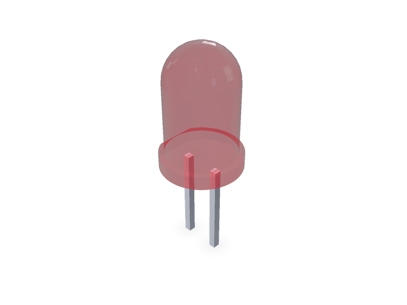
Through-hole round LEDs from Vishay's drawings: 5 mm (T-1 3/4, TLHx5400) and 3 mm (T-1, TLHx4400), red, yellow or green.
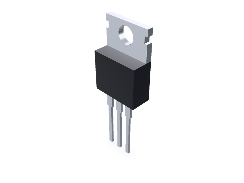
Through-hole TO packages standing on the board: TO-220AB, TO-220AC, TO-220F, TO-262, TO-251AA, TO-247AC, TO-126, TO-92 and the TO-3, TO-18, TO-39 and TO-46 metal cans, from the makers' drawings.
| 1 | """Through-hole transistor packages standing on the board: TO-220AB, TO-220AC, TO-220F, TO-262, TO-251AA, TO-247AC, TO-126, TO-92 (straight |
| 2 | leads) and the TO-3, TO-18, TO-39 and TO-46 metal cans. Lead 1 is at the origin, the leads run along +X, the moulded front faces -Y (TO-92: |
| 3 | the flat face) and the metal tab or pad is at the back (+Y). The board is the XY plane: the leads' shoulders (TO-92: the seating plane; the |
| 4 | cans: the flange) rest on it and the leads go down through it. Dimensions from the makers' package drawings, listed in the README.""" |
| 5 | from steve import Model |
| 6 | import math |
| 7 | |
| 8 | package = "TO-220AB" # TO-220AB, TO-220AC, TO-220F, TO-220F-2, TO-262, TO-251AA, TO-247AC, TO-126, TO-92, TO-3, TO-18, TO-18-2, TO-39 or TO-46 |
| 9 | detail = "full" # full: body, tab and leads; simple: the body and tab only |
| 10 | |
| 11 | # Vishay Siliconix, "TO-220AB (High Voltage)", Package Information, document 92506, revision 30-Sep-2024 (DWG 6031), page 2 table; and |
| 12 | # Vishay Semiconductors, "TO-220AC", Outline Dimensions, document 95221, revision 16-Jan-2026, table: (min, max) in mm, the model uses the |
| 13 | # middle of each. A body+tab thickness, A1 tab thickness, A2 lead's back face to the tab's back, b lead width, b2 shoulder width, |
| 14 | # c lead thickness, D overall height, D1 moulded body height, D2 metal on the back (from the top), E width, E1 back metal width, E2 tab notch |
| 15 | # depth, e1 lead 1 to the last lead, H1 tab above the body, L lead length, L1 shoulder length, P hole diameter, Q hole centre below the top. |
| 16 | TO220AB = dict(A=(4.25, 4.65), A1=(1.20, 1.34), A2=(2.563, 2.92), b=(0.71, 0.91), b2=(1.14, 1.78), c=(0.46, 0.61), D=(14.32, 15.86), |
| 17 | D1=(8.39, 8.79), D2=(12.20, 12.80), E=(9.96, 10.36), E1=(8.14, 8.74), E2=(0.59, 0.69), e1=(5.08, 5.08), H1=(6.30, 6.70), |
| 18 | L=(13.40, 14.40), L1=(3.65, 4.05), P=(3.60, 3.80), Q=(2.54, 2.94)) |
| 19 | TO220AC = dict(A=(4.25, 4.65), A1=(1.14, 1.40), A2=(2.56, 2.92), b=(0.69, 1.01), b2=(1.20, 1.73), c=(0.36, 0.61), D=(14.85, 15.25), |
| 20 | D1=(8.38, 9.02), D2=(11.68, 12.88), E=(10.11, 10.51), E1=(6.86, 8.89), E2=(0.76, 0.76), e1=(4.88, 5.28), H1=(5.84, 6.86), |
| 21 | L=(13.52, 14.02), L1=(3.32, 3.82), P=(3.54, 3.73), Q=(2.60, 3.00)) |
| 22 | # Vishay Siliconix, "TO-247AC (High Voltage)", Package Information, document 91360, revision 07-Sep-2026, version 1 (facility code 9), |
| 23 | # table (nominal) in mm: A body thickness, A1 back face to the leads' back face, A2 exposed copper (drawn at the back face), b lead width, |
| 24 | # b2 outer shoulders, b4 middle shoulder, c lead thickness, D height, D1 x E1 the exposed copper, D2 its top below the top, E width, E2 side |
| 25 | # slot width, e pitch, L lead length, L1 shoulder length, P hole diameter, P1 copper ring round the hole (ref), Q hole and slots below the top. |
| 26 | TO247AC = dict(A=5.02, A1=2.41, A2=1.27, b=1.20, b2=2.00, b4=3.00, c=0.50, D=20.55, D1=16.76, D2=0.66, E=15.70, E1=14.02, E2=4.91, |
| 27 | e=5.46, L=15.15, L1=4.06, P=3.61, P1=7.19, Q=5.50) |
| 28 | # Texas Instruments, LP0003A "TO-92 - 5.34 mm max height", drawing 4215214/C 04/2025 (ti.com/lit/pdf/msot002), straight lead option: |
| 29 | # (min, max) in mm, the model uses the middle: W body width, H body height, T body depth (round back to flat face), K round back to the leads' |
| 30 | # centre line, F flat face width (min), b lead width, c lead thickness, e pitch (1.27 +/-0.13), L lead length (12.7 min), S the seating plane |
| 31 | # below the body ((1.5) typical, reference). |
| 32 | TO92 = dict(W=(4.44, 5.21), H=(4.32, 5.34), T=(3.17, 4.19), K=(2.03, 2.67), F=(3.43, 3.43), b=(0.38, 0.55), c=(0.35, 0.43), e=(1.27, 1.27), |
| 33 | L=(12.7, 12.7), S=(1.5, 1.5)) |
| 34 | # Central Semiconductor, "Package Details - TO-18" (REV: R1; R0 21-June 2004) and "TO-18 2-Lead Case" (REV: R0; 13-March 2013), table |
| 35 | # (min, max) in mm, the model uses the middle (C: its max, the only value; E: 12.70 min): A flange Ø, B can Ø, C flange thickness, D height, |
| 36 | # E lead length, F lead Ø, G lead circle Ø (3 leads) or lead spacing (2 leads), H lead 2 off the line of leads 1 and 3, I tab width, |
| 37 | # J tab length (read as beyond the flange's edge); the tab is at 45 deg, beside lead 1. |
| 38 | TO18 = dict(A=(5.31, 5.84), B=(4.52, 4.95), C=(0.76, 0.76), D=(4.32, 5.33), E=(12.70, 12.70), F=(0.41, 0.48), G=(2.54, 2.54), H=(1.27, 1.27), |
| 39 | I=(0.91, 1.17), J=(0.71, 1.22)) |
| 40 | # Proportions, for looks (README): the TO-220 tab's side notches are 1.4 high, from 1.4 to 2.8 below the top (as drawn); the TO-220AC's cut-off middle lead isn't |
| 41 | # modelled; the TO-247's side slots are half-round (Ø E2) and the copper ring P1 isn't modelled; the TO-92's flat face is cut from a round body |
| 42 | # W across; every lead's shoulder narrows to the lead in one step. |
| 43 | NOTCH = (1.4, 2.8) |
| 44 | # Central Semiconductor, "Package Details - TO-39" (REV R1, R0 21-June 2004) and "Package Details - TO-46" (REV R2, R0 17-July 2008), tables |
| 45 | # (min, max) in mm, the letters as TO18's (C: the max, the only value; E: 12.70 min). TO-46's sheet names the tab width J and its length K; |
| 46 | # here they are I and J, as on the TO-18 and TO-39 sheets. |
| 47 | TO39 = dict(A=(8.51, 9.40), B=(8.00, 8.51), C=(1.02, 1.02), D=(6.10, 6.60), E=(12.70, 12.70), F=(0.41, 0.53), G=(5.08, 5.08), H=(2.54, 2.54), |
| 48 | I=(0.71, 0.86), J=(0.74, 1.14)) |
| 49 | TO46 = dict(A=(5.31, 5.84), B=(4.52, 4.95), C=(1.02, 1.02), D=(1.65, 2.16), E=(12.70, 12.70), F=(0.41, 0.53), G=(2.54, 2.54), H=(1.27, 1.27), |
| 50 | I=(0.91, 1.17), J=(0.71, 1.22)) |
| 51 | CANS = {"TO-18": TO18, "TO-18-2": TO18, "TO-39": TO39, "TO-46": TO46} |
| 52 | # Central Semiconductor, "Package Details - TO-126" (REV R3, R0 21-June 2004), table (min, max) in mm, the middle (single values as given): |
| 53 | # A body thickness, B the leads' centre plane from the back, C lead thickness, D width, E hole centre below the top, F hole diameter, |
| 54 | # G body height, H lead length below the body (shoulder included), J lead width, K pitch, L lead 1 to lead 3, M shoulder width, N shoulder |
| 55 | # length. The back carries the mounting plate ("Mounting Plate Common to Pin 2"). |
| 56 | TO126 = dict(A=(2.40, 2.80), B=(1.27, 1.27), C=(0.38, 0.75), D=(7.40, 8.50), E=(3.75, 3.75), F=(3.00, 3.40), G=(10.50, 12.00), |
| 57 | H=(15.70, 15.70), J=(0.62, 0.90), K=(2.25, 2.25), L=(4.50, 4.50), M=(1.14, 1.40), N=(2.10, 2.10)) |
| 58 | # Central Semiconductor, "Package Details - TO-220FP Case" (REV R5, R2 06-June 2023) and "TO-220FP-2 Case" (REV R2, R0 28-January 2015), |
| 59 | # tables (min, max) in mm; where a sheet gives only a maximum the model uses it. A body thickness, B the thinner top part's thickness, |
| 60 | # C the leads' centre plane from the back, D lead thickness, E width, F the thin top part's height, G body height, H shoulder length, |
| 61 | # J lead length below the body, K lead width, L pitch (TO-220FP-2: each lead's offset from the centre line), M hole centre below the top, |
| 62 | # N hole diameter, P shoulder width. The fully moulded body has no exposed metal. |
| 63 | TO220F = dict(A=(4.20, 5.12), B=(2.30, 3.30), C=(2.50, 3.10), D=(0.80, 0.80), E=(9.70, 10.63), F=(6.06, 7.00), G=(14.80, 16.25), |
| 64 | H=(4.50, 4.50), J=(12.78, 13.80), K=(0.50, 0.90), L=(2.54, 2.54), M=(2.55, 3.55), N=(2.95, 3.40), P=(1.00, 1.47)) |
| 65 | TO220F2 = dict(A=(4.80, 4.80), B=(3.12, 3.12), C=(2.50, 2.90), D=(0.81, 0.81), E=(10.31, 10.31), F=(6.30, 6.90), G=(14.80, 15.40), |
| 66 | H=(4.10, 4.10), J=(13.00, 13.80), K=(0.90, 0.90), L=(2.55, 2.55), M=(2.55, 2.85), N=(3.00, 3.40), P=(1.40, 1.40)) |
| 67 | # Proportions, for looks: the TO-126's mounting plate on the back is 0.3 thick, set in 0.08 x the width from the sides and the top and |
| 68 | # ending 0.1 x the height above the bottom (drawn dashed in the front view, not dimensioned); the TO-220FP-2's cut-off middle lead stub |
| 69 | # (O, P, Q on its sheet) isn't modelled. |
| 70 | PLATE_T = 0.3 |
| 71 | # Vishay Siliconix, "I2PAK (TO-262) (High Voltage)", Package Information, document 91367, revision 27-Oct-08 (DWG 5977), table (min, max) |
| 72 | # in mm, the middle (a single value where the table gives only a min or a max: D1, E1 min; L1 max). A body thickness, A1 the leads' back face |
| 73 | # to the back, b lead width, b2 shoulder width, c lead thickness, c2 tab thickness, D body height, D1 x E1 the thermal pad on the back, |
| 74 | # E width, e pitch, L lead length below the body, L1 the tab above the body, L2 shoulder length. |
| 75 | TO262 = dict(A=(4.06, 4.83), A1=(2.03, 3.02), b=(0.51, 0.99), b2=(1.14, 1.78), c=(0.38, 0.74), c2=(1.14, 1.65), D=(8.38, 9.65), D1=(6.86, 6.86), |
| 76 | E=(9.65, 10.67), E1=(6.22, 6.22), e=(2.54, 2.54), L=(13.46, 14.10), L1=(1.65, 1.65), L2=(3.56, 3.71)) |
| 77 | # Proportions, for looks: the TO-262 tab above the body is the body's width with its top corners chamfered 0.04 x the width (drawn, not |
| 78 | # dimensioned), and the thermal pad on the back is flush, from the body's top down. |
| 79 | # Vishay Siliconix, "Case Outline for TO-251AA (High Voltage)", Package Information, document 91362, revision 27-Dec-2021 (ECN E21-0682 |
| 80 | # rev C, DWG 5968), Option 1, page 1 table (min, max) in mm, the middle (a single value where the table gives only a min: D1, E1). A body |
| 81 | # thickness, A1 the leads' back face to the back, b lead width, b2 shoulder width, b4 tab width, c lead thickness, c2 tab thickness, D body |
| 82 | # height, D1 the thermal pad from the tab's top down, E width, E1 the pad's width, e pitch, L lead length below the body, L1 shoulder length |
| 83 | # below the body (the leads narrow from b2 to b there; section C-C is cut inside it), L2 the tab above the body, L3 the zone below the body |
| 84 | # where the lead is uncontrolled (inside L1, not modelled). THETA2: the tab's top corners are chamfered at 25 to 35 deg (the middle, 30). |
| 85 | TO251AA = dict(A=(2.18, 2.39), A1=(0.89, 1.14), b=(0.64, 0.89), b2=(0.76, 1.14), b4=(4.95, 5.46), c=(0.46, 0.61), c2=(0.46, 0.86), |
| 86 | D=(5.97, 6.22), D1=(5.21, 5.21), E=(6.35, 6.73), E1=(4.32, 4.32), e=(2.29, 2.29), L=(8.89, 9.65), L1=(1.91, 2.29), |
| 87 | L2=(0.89, 1.27), L3=(1.14, 1.52)) |
| 88 | THETA2 = (25, 35) |
| 89 | # Proportions, for looks: the TO-251AA tab's corner chamfers drop a third of L2 (as drawn); the moulding's ejector mark, the body's draft and |
| 90 | # the lead tips' taper aren't modelled. |
| 91 | CHAMFER_DROP = 1 / 3 |
| 92 | # Central Semiconductor, "Package Details - TO-3" (REV R2, R0 9-April 2009), table (min, max) in mm, the middle: A flange length, B can |
| 93 | # diameter, C height above the flange's underside, D lead length below it, E flange thickness, F lead diameter, G mounting holes apart, |
| 94 | # H the leads' line to the far hole, J lead 1 to lead 2, K lead 2 to the holes' axis, L hole diameter, M flange width. The drawing's lower |
| 95 | # view is from below (the can dashed): turned to look from above, with lead 2 along +X from lead 1, the far hole is toward +Y. |
| 96 | TO3 = dict(A=(38.50, 39.96), B=(19.00, 22.23), C=(6.35, 11.43), D=(11.00, 13.10), E=(1.38, 1.65), F=(0.90, 1.15), G=(29.90, 30.40), |
| 97 | H=(16.50, 17.30), J=(10.67, 11.18), K=(5.21, 5.72), L=(3.84, 4.36), M=(25.00, 26.67)) |
| 98 | # Proportions, for looks: the flange outline is read as drawn, round the holes ((A - G) / 2 radius) and round the centre (diameter M) |
| 99 | # joined by tangent lines; the can's top edge is rounded 0.08 x B (drawn, not dimensioned). |
| 100 | CAN_ROUND = 0.08 |
| 101 | # The cans are drawn steel shells, closed at the top and open into the header. No sheet gives the wall, so it is fitted to the can's mass on |
| 102 | # Central's material sheets (TO-3 R3 20-September 2018: 2,550 mg; TO-18 R4 10-February 2020: 114.99 mg; TO-39 R4 16-July 2018: 350 mg; |
| 103 | # TO-46 R2 16-July 2018: 109.313 mg), at the model's density (iron 7.87, steel 7.85), rounded to 0.01 mm. A proportion, not a drawn size. |
| 104 | CAN_WALL = {"TO-3": 0.44, "TO-18": 0.20, "TO-39": 0.25, "TO-46": 0.70} |
| 105 | |
| 106 | PACKAGES = ("TO-220AB", "TO-220AC", "TO-220F", "TO-220F-2", "TO-262", "TO-251AA", "TO-247AC", "TO-126", "TO-92", "TO-3", "TO-18", "TO-18-2", |
| 107 | "TO-39", "TO-46") |
| 108 | if package not in PACKAGES: |
| 109 | raise ValueError("package: " + ", ".join(PACKAGES)) |
| 110 | |
| 111 | |
| 112 | def mid(table): |
| 113 | return {k: (v[0] + v[1]) / 2 if isinstance(v, tuple) else v for k, v in table.items()} |
| 114 | |
| 115 | |
| 116 | model = Model() |
| 117 | |
| 118 | |
| 119 | def box(fid, x0, x1, y0, y1, z0, z1, body, op, name): |
| 120 | model.plane(f"{fid}_plane", on="XY", offset=z0, name=name) |
| 121 | with model.sketch(f"{fid}_sketch", on=f"{fid}_plane", name=name) as sk: |
| 122 | sk.rect(f"{fid}_rect", (x0, y0), (x1, y1)) |
| 123 | model.extrude(fid, f"{fid}_sketch", distance=z1 - z0, op=op, body=body, name=name) |
| 124 | |
| 125 | |
| 126 | def through_y(fid, profile, y0, y1, body, op, name): |
| 127 | """A prism of `profile` (x, z points, or a circle (x, z, r)) from y0 to y1 (y0 > y1: an XZ plane at y0 extrudes along -Y).""" |
| 128 | model.plane(f"{fid}_plane", on="XZ", offset=-y0, name=name) |
| 129 | with model.sketch(f"{fid}_sketch", on=f"{fid}_plane", name=name) as sk: |
| 130 | if len(profile) == 3 and not isinstance(profile[0], tuple): |
| 131 | sk.circle(f"{fid}_circle", (profile[0], profile[1]), profile[2]) |
| 132 | else: |
| 133 | sk.polyline(f"{fid}_outline", profile, closed=True) |
| 134 | model.extrude(fid, f"{fid}_sketch", distance=y0 - y1, op=op, body=body, name=name) |
| 135 | |
| 136 | |
| 137 | def can_shell(fid, x, y, z0, zt, R, t, r, name): |
| 138 | """A can revolved about the vertical axis at (x, y): radius R from z0 to zt, wall t, closed at the top (its edge rounded r) and open at |
| 139 | the bottom.""" |
| 140 | if r > 0: |
| 141 | ri = max(r - t, 0.0) |
| 142 | arc = [(R - r + r * math.cos(math.pi / 2 * k / 8), zt - r + r * math.sin(math.pi / 2 * k / 8)) for k in range(9)] |
| 143 | inner = [(R - t - ri + ri * math.cos(math.pi / 2 * k / 8), zt - t - ri + ri * math.sin(math.pi / 2 * k / 8)) for k in range(9)] |
| 144 | else: |
| 145 | arc, inner = [(R, zt)], [(R - t, zt - t)] |
| 146 | sec = [(R - t, z0), (R, z0)] + arc + [(0.0, zt), (0.0, zt - t)] + inner[::-1] |
| 147 | model.plane(f"{fid}_plane", on="XZ", offset=-y, name=name) |
| 148 | with model.sketch(f"{fid}_sketch", on=f"{fid}_plane", name=name) as sk: |
| 149 | sk.polyline(f"{fid}_section", [(x + u, z) for u, z in sec], closed=True) |
| 150 | model.revolve(fid, f"{fid}_sketch", axis=((x, y, 0.0), (0.0, 0.0, 1.0)), op="new", body=f"{fid}_body", name=name) |
| 151 | |
| 152 | |
| 153 | def leads(xs, b, c, L, shoulder, widths, top): |
| 154 | """Each lead: its shoulder (width from `widths`) from the body's underside `top` down `shoulder`, then the lead (b x c) to L below it.""" |
| 155 | model.plane("leads_plane", on="XY", offset=top - L, name="Leads") |
| 156 | with model.sketch("leads_sketch", on="leads_plane", name="Leads") as sk: |
| 157 | for i, x in enumerate(xs): |
| 158 | sk.rect(f"lead_{i}", (x - b / 2, -c / 2), (x + b / 2, c / 2)) |
| 159 | model.extrude("leads", "leads_sketch", distance=L - shoulder, op="new", body="leads_body", name="Leads") |
| 160 | model.plane("shoulders_plane", on="XY", offset=top - shoulder, name="Lead shoulders") |
| 161 | with model.sketch("shoulders_sketch", on="shoulders_plane", name="Lead shoulders") as sk: |
| 162 | for i, (x, w) in enumerate(zip(xs, widths)): |
| 163 | sk.rect(f"shoulder_{i}", (x - w / 2, -c / 2), (x + w / 2, c / 2)) |
| 164 | model.extrude("shoulders", "shoulders_sketch", distance=shoulder, op="join", body="leads_body", name="Lead shoulders") |
| 165 | |
| 166 | |
| 167 | bodies = {} |
| 168 | if package in ("TO-220AB", "TO-220AC"): |
| 169 | t = mid(TO220AB if package == "TO-220AB" else TO220AC) |
| 170 | xs = [0.0, t["e1"] / 2, t["e1"]] if package == "TO-220AB" else [0.0, t["e1"]] |
| 171 | cx = t["e1"] / 2 |
| 172 | back = t["c"] / 2 + t["A2"] |
| 173 | front = back - t["A"] |
| 174 | z0 = t["L1"] # the shoulders rest on the board |
| 175 | top = z0 + t["D"] |
| 176 | E, E1 = t["E"], t["E1"] |
| 177 | # Moulded body, with the back recessed where the metal shows (E1 wide, from the body's top down to D2 below the package's top). |
| 178 | box("body", cx - E / 2, cx + E / 2, front, back, z0, z0 + t["D1"], "body_body", "new", "Body") |
| 179 | box("back_recess", cx - E1 / 2, cx + E1 / 2, back - t["A1"], back, top - t["D2"], z0 + t["D1"], "body_body", "cut", "Back metal recess") |
| 180 | # Metal tab: E wide above the body, E1 wide down the back; side notches E2 deep at the hole; the hole P at Q below the top. |
| 181 | box("tab", cx - E / 2, cx + E / 2, back - t["A1"], back, z0 + t["D1"], top, "tab_body", "new", "Tab") |
| 182 | box("tab_back", cx - E1 / 2, cx + E1 / 2, back - t["A1"], back, top - t["D2"], z0 + t["D1"], "tab_body", "join", "Tab") |
| 183 | zq = top - t["Q"] |
| 184 | for side, x0 in (("left", cx - E / 2), ("right", cx + E / 2 - t["E2"])): |
| 185 | box(f"notch_{side}", x0, x0 + t["E2"], back - t["A1"], back, top - NOTCH[1], top - NOTCH[0], "tab_body", "cut", "Tab notch") |
| 186 | through_y("tab_hole", (cx, zq, t["P"] / 2), back + 0.1, back - t["A1"] - 0.1, "tab_body", "cut", "Mounting hole") |
| 187 | bodies = {"body_body": ("pa6", "#1c1c1e"), "tab_body": ("copper", "#c8ccd0")} |
| 188 | if detail == "full": |
| 189 | leads(xs, t["b"], t["c"], t["L"], t["L1"], [t["b2"]] * len(xs), z0) |
| 190 | elif package == "TO-262": |
| 191 | # Moulded body with the metal tab: c2 thick, flush with the back, showing as the pad D1 x E1 from the body's top down and rising L1 above it. |
| 192 | t = mid(TO262) |
| 193 | xs = [0.0, t["e"], 2 * t["e"]] |
| 194 | cx = t["e"] |
| 195 | back = t["c"] / 2 + t["A1"] |
| 196 | front = back - t["A"] |
| 197 | z0 = t["L2"] # the shoulders rest on the board |
| 198 | top = z0 + t["D"] |
| 199 | E, k = t["E"], 0.04 * t["E"] |
| 200 | box("body", cx - E / 2, cx + E / 2, front, back, z0, top, "body_body", "new", "Body") |
| 201 | box("pad_recess", cx - t["E1"] / 2, cx + t["E1"] / 2, back - t["c2"], back, top - t["D1"], top, "body_body", "cut", "Thermal pad recess") |
| 202 | box("pad", cx - t["E1"] / 2, cx + t["E1"] / 2, back - t["c2"], back, top - t["D1"], top, "tab_body", "new", "Thermal pad") |
| 203 | through_y("tab_top", [(cx - E / 2, top), (cx + E / 2, top), (cx + E / 2, top + t["L1"] - k), (cx + E / 2 - k, top + t["L1"]), |
| 204 | (cx - E / 2 + k, top + t["L1"]), (cx - E / 2, top + t["L1"] - k)], back, back - t["c2"], "tab_body", "join", "Tab") |
| 205 | bodies = {"body_body": ("pa6", "#1c1c1e"), "tab_body": ("copper", "#c8ccd0")} |
| 206 | if detail == "full": |
| 207 | leads(xs, t["b"], t["c"], t["L"], t["L2"], [t["b2"]] * 3, z0) |
| 208 | elif package == "TO-251AA": |
| 209 | # Moulded body with the metal tab: c2 thick, flush with the back, showing as the thermal pad E1 wide from D1 below the tab's top up to |
| 210 | # the body's top, and rising L2 above the body b4 wide, its top corners chamfered at THETA2. |
| 211 | t = mid(TO251AA) |
| 212 | xs = [0.0, t["e"], 2 * t["e"]] |
| 213 | cx = t["e"] |
| 214 | back = t["c"] / 2 + t["A1"] |
| 215 | front = back - t["A"] |
| 216 | z0 = t["L1"] # the shoulders rest on the board |
| 217 | top = z0 + t["D"] |
| 218 | E, w = t["E"], t["b4"] / 2 |
| 219 | box("body", cx - E / 2, cx + E / 2, front, back, z0, top, "body_body", "new", "Body") |
| 220 | pad0 = top + t["L2"] - t["D1"] |
| 221 | box("pad_recess", cx - t["E1"] / 2, cx + t["E1"] / 2, back - t["c2"], back, pad0, top, "body_body", "cut", "Thermal pad recess") |
| 222 | box("pad", cx - t["E1"] / 2, cx + t["E1"] / 2, back - t["c2"], back, pad0, top, "tab_body", "new", "Thermal pad") |
| 223 | dz = CHAMFER_DROP * t["L2"] |
| 224 | dx = dz / math.tan(math.radians(sum(THETA2) / 2)) |
| 225 | through_y("tab_top", [(cx - w, top), (cx + w, top), (cx + w, top + t["L2"] - dz), (cx + w - dx, top + t["L2"]), |
| 226 | (cx - w + dx, top + t["L2"]), (cx - w, top + t["L2"] - dz)], back, back - t["c2"], "tab_body", "join", "Tab") |
| 227 | bodies = {"body_body": ("pa6", "#1c1c1e"), "tab_body": ("copper", "#c8ccd0")} |
| 228 | if detail == "full": |
| 229 | leads(xs, t["b"], t["c"], t["L"], t["L1"], [t["b2"]] * 3, z0) |
| 230 | elif package == "TO-3": |
| 231 | # Flange (header) on the board, holes along Y; the can on it; lead 1 at the origin, lead 2 J along +X, the holes' axis K back from |
| 232 | # lead 2 and the far hole H from the leads' line. |
| 233 | t = mid(TO3) |
| 234 | hx = t["J"] - t["K"] |
| 235 | yc = t["H"] - t["G"] / 2 |
| 236 | re_, R = (t["A"] - t["G"]) / 2, t["M"] / 2 |
| 237 | circles = [(hx, yc - t["G"] / 2, re_), (hx, yc, R), (hx, yc + t["G"] / 2, re_)] |
| 238 | pts = sorted({(round(x + r * math.cos(2 * math.pi * k / 144), 4), round(y + r * math.sin(2 * math.pi * k / 144), 4)) |
| 239 | for x, y, r in circles for k in range(144)}) |
| 240 | |
| 241 | def cross(o, a, b): |
| 242 | return (a[0] - o[0]) * (b[1] - o[1]) - (a[1] - o[1]) * (b[0] - o[0]) |
| 243 | |
| 244 | hull = [] |
| 245 | for seq in (pts, pts[::-1]): # Andrew's monotone chain: lower then upper hull |
| 246 | part = [] |
| 247 | for p in seq: |
| 248 | while len(part) >= 2 and cross(part[-2], part[-1], p) <= 0: |
| 249 | part.pop() |
| 250 | part.append(p) |
| 251 | hull += part[:-1] |
| 252 | model.plane("flange_plane", on="XY", offset=0.0, name="Flange") |
| 253 | with model.sketch("flange_sketch", on="flange_plane", name="Flange") as sk: |
| 254 | sk.polyline("flange_outline", hull, closed=True) |
| 255 | model.extrude("flange", "flange_sketch", distance=t["E"], op="new", body="header_body", name="Flange") |
| 256 | model.plane("holes_plane", on="XY", offset=-0.1, name="Mounting holes") |
| 257 | with model.sketch("holes_sketch", on="holes_plane", name="Mounting holes") as sk: |
| 258 | for i, s_ in enumerate((-1, 1)): |
| 259 | sk.circle(f"hole_{i}", (hx, yc + s_ * t["G"] / 2), t["L"] / 2) |
| 260 | model.extrude("holes", "holes_sketch", distance=t["E"] + 0.2, op="cut", body="header_body", name="Mounting holes") |
| 261 | # The can: a shell Ø B from the flange's top to C, its top edge rounded. |
| 262 | can_shell("can", hx, yc, t["E"], t["C"], t["B"] / 2, CAN_WALL["TO-3"], CAN_ROUND * t["B"], "Can") |
| 263 | bodies = {"header_body": ("iron", "#c9ccd1"), "can_body": ("iron", "#d5d8dc")} |
| 264 | if detail == "full": |
| 265 | model.plane("leads_plane", on="XY", offset=-t["D"], name="Leads") |
| 266 | with model.sketch("leads_sketch", on="leads_plane", name="Leads") as sk: |
| 267 | for i, x in enumerate((0.0, t["J"])): |
| 268 | sk.circle(f"lead_{i}", (x, 0.0), t["F"] / 2) |
| 269 | model.extrude("leads", "leads_sketch", distance=t["D"], op="new", body="leads_body", name="Leads") |
| 270 | elif package in ("TO-220F", "TO-220F-2"): |
| 271 | # Fully moulded (no exposed metal): the full thickness A up to F below the top, then the thinner top part B thick, its back face flush. |
| 272 | t = mid(TO220F if package == "TO-220F" else TO220F2) |
| 273 | xs = [0.0, t["L"], 2 * t["L"]] if package == "TO-220F" else [0.0, 2 * t["L"]] |
| 274 | cx = xs[-1] / 2 |
| 275 | back = t["C"] |
| 276 | front = back - t["A"] |
| 277 | z0 = t["H"] # the shoulders rest on the board |
| 278 | top = z0 + t["G"] |
| 279 | E = t["E"] |
| 280 | box("body", cx - E / 2, cx + E / 2, front, back, z0, top - t["F"], "body_body", "new", "Body") |
| 281 | box("body_top", cx - E / 2, cx + E / 2, back - t["B"], back, top - t["F"], top, "body_body", "join", "Body") |
| 282 | through_y("hole", (cx, top - t["M"], t["N"] / 2), back + 0.1, back - t["B"] - 0.1, "body_body", "cut", "Mounting hole") |
| 283 | bodies = {"body_body": ("pa6", "#1c1c1e")} |
| 284 | if detail == "full": |
| 285 | leads(xs, t["K"], t["D"], t["J"], t["H"], [t["P"]] * len(xs), z0) |
| 286 | elif package == "TO-126": |
| 287 | # Moulded body with the mounting plate on its back and the hole through both; leads at pitch K, their centre plane B in front of the back. |
| 288 | t = mid(TO126) |
| 289 | xs = [0.0, t["K"], 2 * t["K"]] |
| 290 | cx = t["K"] |
| 291 | back = t["B"] |
| 292 | front = back - t["A"] |
| 293 | z0 = t["N"] |
| 294 | top = z0 + t["G"] |
| 295 | W = t["D"] |
| 296 | box("body", cx - W / 2, cx + W / 2, front, back, z0, top, "body_body", "new", "Body") |
| 297 | m = 0.08 * W |
| 298 | box("plate_recess", cx - W / 2 + m, cx + W / 2 - m, back - PLATE_T, back, z0 + 0.1 * t["G"], top - m, "body_body", "cut", "Plate recess") |
| 299 | box("plate", cx - W / 2 + m, cx + W / 2 - m, back - PLATE_T, back, z0 + 0.1 * t["G"], top - m, "plate_body", "new", "Mounting plate") |
| 300 | through_y("hole", (cx, top - t["E"], t["F"] / 2), back + 0.1, front - 0.1, "body_body", "cut", "Mounting hole") |
| 301 | through_y("plate_hole", (cx, top - t["E"], t["F"] / 2), back + 0.1, front - 0.1, "plate_body", "cut", "Mounting hole") |
| 302 | bodies = {"body_body": ("pa6", "#1c1c1e"), "plate_body": ("copper", "#c8ccd0")} |
| 303 | if detail == "full": |
| 304 | leads(xs, t["J"], t["C"], t["H"], t["N"], [t["M"]] * 3, z0) |
| 305 | elif package == "TO-247AC": |
| 306 | t = TO247AC |
| 307 | xs = [0.0, t["e"], 2 * t["e"]] |
| 308 | cx = t["e"] |
| 309 | back = t["c"] / 2 + t["A1"] |
| 310 | front = back - t["A"] |
| 311 | z0 = t["L1"] |
| 312 | top = z0 + t["D"] |
| 313 | E = t["E"] |
| 314 | box("body", cx - E / 2, cx + E / 2, front, back, z0, top, "body_body", "new", "Body") |
| 315 | zq = top - t["Q"] |
| 316 | for side, x in (("left", cx - E / 2), ("right", cx + E / 2)): |
| 317 | through_y(f"slot_{side}", (x, zq, t["E2"] / 2), back + 0.1, front - 0.1, "body_body", "cut", "Side slot") |
| 318 | # Exposed copper on the back, flush: D1 x E1 from D2 below the top, A2 thick, with the hole through it. |
| 319 | box("pad_recess", cx - t["E1"] / 2, cx + t["E1"] / 2, back - t["A2"], back, top - t["D2"] - t["D1"], top - t["D2"], "body_body", "cut", "Copper recess") |
| 320 | box("pad", cx - t["E1"] / 2, cx + t["E1"] / 2, back - t["A2"], back, top - t["D2"] - t["D1"], top - t["D2"], "pad_body", "new", "Exposed copper") |
| 321 | through_y("hole", (cx, zq, t["P"] / 2), back + 0.1, front - 0.1, "body_body", "cut", "Mounting hole") |
| 322 | through_y("pad_hole", (cx, zq, t["P"] / 2), back + 0.1, front - 0.1, "pad_body", "cut", "Mounting hole") |
| 323 | for side, x in (("left", cx - E / 2), ("right", cx + E / 2)): |
| 324 | through_y(f"pad_slot_{side}", (x, zq, t["E2"] / 2), back + 0.1, front - 0.1, "pad_body", "cut", "Side slot") |
| 325 | bodies = {"body_body": ("pa6", "#1c1c1e"), "pad_body": ("copper", "#c8ccd0")} |
| 326 | if detail == "full": |
| 327 | leads(xs, t["b"], t["c"], t["L"], t["L1"], [t["b2"], t["b4"], t["b2"]], z0) |
| 328 | elif package in CANS: |
| 329 | # Metal can: the flange (header) on the board, the can on it; leads on a circle round the axis (lead 1 at the origin, lead 3 or lead 2 |
| 330 | # at +X by G, the 3-lead part's lead 2 H off that line along -Y); the tab at 45 deg toward -X +Y, beside lead 1. |
| 331 | t = mid(CANS[package]) |
| 332 | cx = t["G"] / 2 |
| 333 | xs = [(0.0, 0.0), (t["G"], 0.0)] if package == "TO-18-2" else [(0.0, 0.0), (cx, -t["H"]), (t["G"], 0.0)] |
| 334 | model.plane("flange_plane", on="XY", offset=0.0, name="Flange") |
| 335 | with model.sketch("flange_sketch", on="flange_plane", name="Flange") as sk: |
| 336 | sk.circle("flange_round", (cx, 0.0), t["A"] / 2) |
| 337 | u = (-math.sqrt(0.5), math.sqrt(0.5)) |
| 338 | v = (u[1], -u[0]) |
| 339 | r0, r1, w = t["A"] / 2 - 0.3, t["A"] / 2 + t["J"], t["I"] / 2 |
| 340 | sk.polyline("tab_outline", [(cx + u[0] * r + v[0] * s, u[1] * r + v[1] * s) for r, s in ((r0, -w), (r1, -w), (r1, w), (r0, w))], closed=True) |
| 341 | model.extrude("flange", "flange_sketch", distance=t["C"], op="new", body="header_body", name="Flange and tab") |
| 342 | can_shell("can", cx, 0.0, t["C"], t["D"], t["B"] / 2, CAN_WALL[package[:5]], 0.0, "Can") |
| 343 | bodies = {"header_body": ("nickel", "#c9ccd1"), "can_body": ("steel-dc01", "#d5d8dc")} |
| 344 | if detail == "full": |
| 345 | model.plane("leads_plane", on="XY", offset=-t["E"], name="Leads") |
| 346 | with model.sketch("leads_sketch", on="leads_plane", name="Leads") as sk: |
| 347 | for i, (x, y) in enumerate(xs): |
| 348 | sk.circle(f"lead_{i}", (x, y), t["F"] / 2) |
| 349 | model.extrude("leads", "leads_sketch", distance=t["E"], op="new", body="leads_body", name="Leads") |
| 350 | else: |
| 351 | t = mid(TO92) |
| 352 | xs = [0.0, t["e"], 2 * t["e"]] |
| 353 | cx = t["e"] |
| 354 | R = t["W"] / 2 |
| 355 | yc = t["K"] - R # the round body's axis: K from the round back to the leads, so the back is at +K |
| 356 | flat = t["K"] - t["T"] # the flat face (-Y) |
| 357 | z0 = t["S"] |
| 358 | n = 24 |
| 359 | a0 = math.asin(max(-1.0, min(1.0, (flat - yc) / R))) |
| 360 | pts = [(cx + R * math.cos(a), yc + R * math.sin(a)) for a in (a0 + (math.pi - 2 * a0) * k / n for k in range(n + 1))] |
| 361 | model.plane("body_plane", on="XY", offset=z0, name="Body") |
| 362 | with model.sketch("body_sketch", on="body_plane", name="Body") as sk: |
| 363 | sk.polyline("body_outline", [(cx + R * math.cos(a0), flat)] + pts[1:-1] + [(cx - R * math.cos(a0), flat)], closed=True) |
| 364 | model.extrude("body", "body_sketch", distance=t["H"], op="new", body="body_body", name="Body") |
| 365 | bodies = {"body_body": ("pa6", "#1c1c1e")} |
| 366 | if detail == "full": |
| 367 | model.plane("leads_plane", on="XY", offset=z0 - t["L"], name="Leads") |
| 368 | with model.sketch("leads_sketch", on="leads_plane", name="Leads") as sk: |
| 369 | for i, x in enumerate(xs): |
| 370 | sk.rect(f"lead_{i}", (x - t["b"] / 2, -t["c"] / 2), (x + t["b"] / 2, t["c"] / 2)) |
| 371 | model.extrude("leads", "leads_sketch", distance=t["L"], op="new", body="leads_body", name="Leads") |
| 372 | if detail == "full": |
| 373 | bodies["leads_body"] = ("nickel", "#d8c58a") if package in CANS else ("iron", "#d9dadc") if package == "TO-3" else ("copper", "#c9ccd1") |
| 374 | # Materials, for looks and a rough mass: the moulding is epoxy (nylon, PA6, the nearest in the list), the tab and pad copper (nickel or tin |
| 375 | # plated), the leads tinned copper. TO-18 (Central's material sheets): the header and leads Kovar (density 8.36; nickel, 8.9, is the nearest |
| 376 | # in the list), the can a nickel-plated iron alloy (steel). TO-3 (Central's material sheet R3, 20-September 2018): the header and the can |
| 377 | # nickel-plated iron, the terminals tin-plated; the leads are taken as the header's iron. |
| 378 | for body, (material, colour) in bodies.items(): |
| 379 | model.material(material, bodies=[body], color=colour) |
| 380 | result = model.result() |
| 381 |
| 1 | name = "steve/to-package" |
| 2 | version = "1.3.0" |
| 3 | runtime = "steve" |
| 4 | license = "MIT" |
| 5 | summary = "Through-hole TO packages standing on the board: TO-220AB, TO-220AC, TO-220F, TO-262, TO-251AA, TO-247AC, TO-126, TO-92 and the TO-3, TO-18, TO-39 and TO-46 metal cans, from the makers' drawings." |
| 6 | description = """A through-hole transistor, regulator or diode package standing on the board, from the maker's package drawing: TO-220AB, TO-220AC, TO-262 (I2PAK) and TO-251AA (IPAK) with their metal tabs, the fully moulded TO-220F, TO-247AC, TO-126, TO-92 with straight leads, the TO-3 can on its two-hole flange, and the TO-18, TO-39 and TO-46 cans. Lead 1 at the origin, the leads along +X, the moulded front toward -Y. See the README.""" |
| 7 | tags = ["to-220", "to-247", "to-92", "to-3", "to-18", "to-126", "transistor", "package", "through-hole", "electronics"] |
| 8 | |
| 9 | [parameters.package] |
| 10 | type = "choice" |
| 11 | default = "TO-220AB" |
| 12 | choices = ["TO-220AB", "TO-220AC", "TO-220F", "TO-220F-2", "TO-262", "TO-251AA", "TO-247AC", "TO-126", "TO-92", "TO-3", "TO-18", "TO-18-2", "TO-39", "TO-46"] |
| 13 | label = "Package" |
| 14 | description = "TO-220AB: 3 leads at 2.54. TO-220AC: 2 leads 5.08 apart. TO-220F: fully moulded, 3 leads; -2: 2 leads 5.1 apart. TO-262 (I2PAK): 3 leads at 2.54, tab above. TO-251AA (IPAK): 3 leads at 2.29, tab above. TO-247AC: 3 leads at 5.46. TO-126: 3 leads at 2.25. TO-92: 3 straight leads at 1.27. TO-3: can on a flange with 2 holes, 2 leads 10.9 apart. TO-18: can, 3 leads on a 2.54 circle; -2: 2 leads. TO-39: can Ø 9, 3 leads on a 5.08 circle. TO-46: low can, 3 leads." |
| 15 | |
| 16 | [parameters.detail] |
| 17 | type = "choice" |
| 18 | default = "full" |
| 19 | choices = ["full", "simple"] |
| 20 | label = "Detail" |
| 21 | description = "full: body, tab and leads. simple: the body and tab only, for big assemblies." |
| 22 | |
| 23 | [[presets]] |
| 24 | id = "TO-220AB" |
| 25 | title = "TO-220AB, 3 leads, 2.54 pitch, vertical (Vishay outline)" |
| 26 | params = { package = "TO-220AB" } |
| 27 | aliases = ["TO-220-3", "TO-220", "TO-220AB", "JEDEC TO-220AB", "TO220 3 lead"] |
| 28 | standard = "Vishay TO-220AB" |
| 29 | |
| 30 | [[presets]] |
| 31 | id = "TO-220AC" |
| 32 | title = "TO-220AC, 2 leads, 5.08 apart, vertical (Vishay outline)" |
| 33 | params = { package = "TO-220AC" } |
| 34 | aliases = ["TO-220-2", "TO-220AC", "JEDEC TO-220AC", "TO220 2 lead"] |
| 35 | standard = "Vishay TO-220AC" |
| 36 | |
| 37 | [[presets]] |
| 38 | id = "TO-220F" |
| 39 | title = "TO-220F (fully moulded), 3 leads, 2.54 pitch, vertical (Central Semiconductor outline)" |
| 40 | params = { package = "TO-220F" } |
| 41 | aliases = ["TO-220F-3", "TO-220F", "TO-220FP", "TO-220 FullPAK", "TO-220 full pack 3 lead"] |
| 42 | standard = "Central TO-220FP" |
| 43 | |
| 44 | [[presets]] |
| 45 | id = "TO-220F-2" |
| 46 | title = "TO-220F (fully moulded), 2 leads, 5.1 apart, vertical (Central Semiconductor outline)" |
| 47 | params = { package = "TO-220F-2" } |
| 48 | aliases = ["TO-220F-2", "TO-220FP-2", "TO-220 full pack 2 lead"] |
| 49 | standard = "Central TO-220FP-2" |
| 50 | |
| 51 | [[presets]] |
| 52 | id = "TO-262" |
| 53 | title = "TO-262 (I2PAK), 3 leads, 2.54 pitch, vertical (Vishay outline)" |
| 54 | params = { package = "TO-262" } |
| 55 | aliases = ["TO-262-3", "TO-262", "TO-262AA", "I2PAK", "I2-PAK"] |
| 56 | standard = "Vishay TO-262" |
| 57 | |
| 58 | [[presets]] |
| 59 | id = "TO-251AA" |
| 60 | title = "TO-251AA (IPAK), 3 leads, 2.29 pitch, vertical (Vishay outline)" |
| 61 | params = { package = "TO-251AA" } |
| 62 | aliases = ["TO-251-3", "TO-251", "TO-251AA", "JEDEC TO-251AA", "IPAK", "I-PAK"] |
| 63 | standard = "Vishay TO-251AA" |
| 64 | |
| 65 | [[presets]] |
| 66 | id = "TO-247AC" |
| 67 | title = "TO-247AC, 3 leads, 5.46 pitch, vertical (Vishay outline)" |
| 68 | params = { package = "TO-247AC" } |
| 69 | aliases = ["TO-247-3", "TO-247", "TO-247AC", "JEDEC TO-247AC", "TO247 3 lead"] |
| 70 | standard = "Vishay TO-247AC" |
| 71 | |
| 72 | [[presets]] |
| 73 | id = "TO-126" |
| 74 | title = "TO-126, 3 leads, 2.25 pitch, vertical (Central Semiconductor outline)" |
| 75 | params = { package = "TO-126" } |
| 76 | aliases = ["TO-126-3", "TO-126", "TO126 3 lead", "SOT-32"] |
| 77 | standard = "Central TO-126" |
| 78 | |
| 79 | [[presets]] |
| 80 | id = "TO-92" |
| 81 | title = "TO-92, 3 straight leads, 1.27 pitch (TI LP0003A)" |
| 82 | params = { package = "TO-92" } |
| 83 | aliases = ["TO-92-3", "TO-92", "TO-226AA", "JEDEC TO-226AA", "TO92 straight leads", "LP0003A", "TO-92, 3 straight leads, 1.27 pitch (TI LP0003A)"] |
| 84 | standard = "TI LP0003A" |
| 85 | |
| 86 | [[presets]] |
| 87 | id = "TO-3" |
| 88 | title = "TO-3 metal can on a flange, 2 leads (Central Semiconductor outline)" |
| 89 | params = { package = "TO-3" } |
| 90 | aliases = ["TO-3", "TO-204AA", "JEDEC TO-204AA", "TO3 metal can 2 lead"] |
| 91 | standard = "Central TO-3" |
| 92 | |
| 93 | [[presets]] |
| 94 | id = "TO-18" |
| 95 | title = "TO-18 metal can, 3 leads (Central Semiconductor outline)" |
| 96 | params = { package = "TO-18" } |
| 97 | aliases = ["TO-18-3", "TO-18", "TO-206AA", "JEDEC TO-206AA", "TO18 metal can 3 lead"] |
| 98 | standard = "Central TO-18" |
| 99 | |
| 100 | [[presets]] |
| 101 | id = "TO-18-2" |
| 102 | title = "TO-18 metal can, 2 leads (Central Semiconductor outline)" |
| 103 | params = { package = "TO-18-2" } |
| 104 | aliases = ["TO-18-2", "TO-18 2 lead", "TO18 metal can 2 lead"] |
| 105 | standard = "Central TO-18 2-lead" |
| 106 | |
| 107 | [[presets]] |
| 108 | id = "TO-39" |
| 109 | title = "TO-39 metal can, 3 leads (Central Semiconductor outline)" |
| 110 | params = { package = "TO-39" } |
| 111 | aliases = ["TO-39-3", "TO-39", "TO-205AD", "JEDEC TO-205AD", "TO39 metal can 3 lead"] |
| 112 | standard = "Central TO-39" |
| 113 | |
| 114 | [[presets]] |
| 115 | id = "TO-46" |
| 116 | title = "TO-46 metal can, 3 leads (Central Semiconductor outline)" |
| 117 | params = { package = "TO-46" } |
| 118 | aliases = ["TO-46-3", "TO-46", "TO-206AB", "JEDEC TO-206AB", "TO46 metal can 3 lead"] |
| 119 | standard = "Central TO-46" |
| 120 | |
| 121 | [[presets]] |
| 122 | id = "TO-220AB-simple" |
| 123 | title = "TO-220AB, 3 leads, 2.54 pitch, vertical (Vishay outline), simple" |
| 124 | params = { package = "TO-220AB", detail = "simple" } |
| 125 | aliases = ["TO-220AB simple"] |
| 126 | standard = "Vishay TO-220AB" |
| 127 |
A through-hole transistor, regulator or diode package standing on the board, built from the maker's package drawing. These are the JEDEC outlines that every maker builds:
package |
Leads | Body (W x thickness x height) | Source |
|---|---|---|---|
TO-220AB |
3, 2.54 pitch | 10.16 x 4.45 x 15.09 (tab included) | Vishay Siliconix 92506 |
TO-220AC |
2, 5.08 apart | 10.31 x 4.45 x 15.05 (tab included) | Vishay Semiconductors 95221 |
TO-220F |
3, 2.54 pitch | 10.17 x 4.66 x 15.53, fully moulded | Central Semiconductor TO-220FP |
TO-220F-2 |
2, 5.10 apart | 10.31 x 4.80 x 15.10, fully moulded | Central Semiconductor TO-220FP-2 |
TO-262 |
3, 2.54 pitch | 10.16 x 4.45 x 10.67 (tab included) | Vishay Siliconix 91367 |
TO-251AA |
3, 2.29 pitch | 6.54 x 2.29 x 7.18 (tab included) | Vishay Siliconix 91362 |
TO-247AC |
3, 5.46 pitch | 15.70 x 5.02 x 20.55 | Vishay Siliconix 91360 |
TO-126 |
3, 2.25 pitch | 7.95 x 2.60 x 11.25 | Central Semiconductor TO-126 |
TO-92 |
3 straight, 1.27 pitch | 4.83 x 3.68 x 4.83 | TI LP0003A |
TO-3 |
2, 10.93 apart | flange 39.23 x 25.84 with 2 holes 30.15 apart, can Ø 20.62, 8.89 high | Central Semiconductor TO-3 |
TO-18 |
3, on a Ø 2.54 circle | flange Ø 5.58, can Ø 4.74, 4.83 high | Central Semiconductor TO-18 |
TO-18-2 |
2, 2.54 apart | as TO-18 |
Central Semiconductor TO-18 2-Lead |
TO-39 |
3, on a Ø 5.08 circle | flange Ø 8.96, can Ø 8.26, 6.35 high | Central Semiconductor TO-39 |
TO-46 |
3, on a Ø 2.54 circle | flange Ø 5.58, can Ø 4.74, 1.91 high | Central Semiconductor TO-46 |
Lead 1 is at the origin and the leads run along +X. The moulded front faces -Y (on the TO-92, the flat face), and the metal tab, exposed copper or mounting plate is at the back (+Y).
detail = "simple" leaves out the leads.
Each table gives a minimum and a maximum. The part uses the middle of the two, except where noted. part.py holds every table as read.
How the letters are read:
Proportions, for looks only. The drawings show these but don't dimension them:
The reference models were measured against the drawings, and each falls inside the drawing's tolerances:
Added in 1.1.0, measured the same way:
Added in 1.2.0:
Added in 1.3.0:
The names name the JEDEC package, so they map to the maker's drawing of it, with the pitch and lead order as named, and the differences are listed here.
The reference models stand their bodies at different heights above the board: the TO-92 at 2.5, and the TO-18, TO-39 and TO-46 at about 5. The drawings don't give these, so this part uses the drawings' own seating.
So these map: TO-220-3_Vertical (TO-220AB), TO-220-2_Vertical (TO-220AC), TO-247-3_Vertical (TO-247AC), TO-92 and TO-92_Inline (TO-92), TO-18-3 (TO-18), TO-18-2 (TO-18-2), TO-39-3 (TO-39), TO-46-3 (TO-46), TO-126-3_Vertical (TO-126), TO-220F-3_Vertical (TO-220F), TO-220F-2_Vertical (TO-220F-2), TO-262-3_Vertical (TO-262), TO-251-3_Vertical (TO-251AA) and TO-3 (TO-3).
These stay "no table read yet" (COVERAGE.md):
_Wide). TI's formed leads are 2.4 to 2.9 apart, with a land pattern of 2.6.| 1 | # TO package (through-hole) |
| 2 | |
| 3 | A through-hole transistor, regulator or diode package standing on the board, built from the maker's package drawing. These are the JEDEC outlines that every maker builds: |
| 4 | |
| 5 | | `package` | Leads | Body (W x thickness x height) | Source | |
| 6 | |---|---|---|---| |
| 7 | | `TO-220AB` | 3, 2.54 pitch | 10.16 x 4.45 x 15.09 (tab included) | Vishay Siliconix 92506 | |
| 8 | | `TO-220AC` | 2, 5.08 apart | 10.31 x 4.45 x 15.05 (tab included) | Vishay Semiconductors 95221 | |
| 9 | | `TO-220F` | 3, 2.54 pitch | 10.17 x 4.66 x 15.53, fully moulded | Central Semiconductor TO-220FP | |
| 10 | | `TO-220F-2` | 2, 5.10 apart | 10.31 x 4.80 x 15.10, fully moulded | Central Semiconductor TO-220FP-2 | |
| 11 | | `TO-262` | 3, 2.54 pitch | 10.16 x 4.45 x 10.67 (tab included) | Vishay Siliconix 91367 | |
| 12 | | `TO-251AA` | 3, 2.29 pitch | 6.54 x 2.29 x 7.18 (tab included) | Vishay Siliconix 91362 | |
| 13 | | `TO-247AC` | 3, 5.46 pitch | 15.70 x 5.02 x 20.55 | Vishay Siliconix 91360 | |
| 14 | | `TO-126` | 3, 2.25 pitch | 7.95 x 2.60 x 11.25 | Central Semiconductor TO-126 | |
| 15 | | `TO-92` | 3 straight, 1.27 pitch | 4.83 x 3.68 x 4.83 | TI LP0003A | |
| 16 | | `TO-3` | 2, 10.93 apart | flange 39.23 x 25.84 with 2 holes 30.15 apart, can Ø 20.62, 8.89 high | Central Semiconductor TO-3 | |
| 17 | | `TO-18` | 3, on a Ø 2.54 circle | flange Ø 5.58, can Ø 4.74, 4.83 high | Central Semiconductor TO-18 | |
| 18 | | `TO-18-2` | 2, 2.54 apart | as `TO-18` | Central Semiconductor TO-18 2-Lead | |
| 19 | | `TO-39` | 3, on a Ø 5.08 circle | flange Ø 8.96, can Ø 8.26, 6.35 high | Central Semiconductor TO-39 | |
| 20 | | `TO-46` | 3, on a Ø 2.54 circle | flange Ø 5.58, can Ø 4.74, 1.91 high | Central Semiconductor TO-46 | |
| 21 | |
| 22 | Lead 1 is at the origin and the leads run along +X. The moulded front faces -Y (on the TO-92, the flat face), and the metal tab, exposed copper or mounting plate is at the back (+Y). |
| 23 | |
| 24 | - **TO-220, TO-220F, TO-262, TO-251AA, TO-247 and TO-126.** The leads' shoulders rest on the board (the XY plane), and the leads continue their full length down through it. |
| 25 | - **TO-92.** The body sits 1.5 above the board (TI's reference seating plane). |
| 26 | - **TO-3.** The flange sits on the board, its mounting holes on a line along Y. Lead 2 is J along +X from lead 1, the holes' line is K back from lead 2, and the far hole is H from the leads' line, toward +Y. The leads are off the can's centre, as drawn. |
| 27 | - **TO-18, TO-39 and TO-46.** The flange sits on the board. Leads 1 and 3 are G apart along +X (2.54, or 5.08 on the TO-39), and lead 2 is H off that line along -Y (1.27, or 2.54). The tab is at 45°, beside lead 1. |
| 28 | |
| 29 | `detail = "simple"` leaves out the leads. |
| 30 | |
| 31 | ## Source |
| 32 | |
| 33 | Each table gives a minimum and a maximum. The part uses the middle of the two, except where noted. `part.py` holds every table as read. |
| 34 | |
| 35 | - **Vishay Siliconix, "TO-220AB (High Voltage)"**, Package Information, document 92506, revision 30-Sep-2024 (DWG 6031), from vishay.com. |
| 36 | - Page 1, drawing: front, side and back views and section F-F. |
| 37 | - Page 2, table (mm): A 4.25–4.65, A1 1.20–1.34, A2 2.563–2.92, b 0.71–0.91, b2 1.14–1.78, c 0.46–0.61, D 14.32–15.86, D1 8.39–8.79, D2 12.20–12.80, E 9.96–10.36, E1 8.14–8.74, E2 0.59–0.69, e 2.54, e1 5.08, H1 6.30–6.70, L 13.40–14.40, L1 3.65–4.05, ØP 3.60–3.80, Q 2.54–2.94. |
| 38 | - **Vishay Semiconductors, "TO-220AC"**, Outline Dimensions, document 95221, revision 16-Jan-2026, from vishay.com. The drawing and table use the same letters. Here e1 is 4.88–5.28, the spacing of the two leads, and E2 is 0.76 max. The outline conforms to JEDEC TO-220AC. |
| 39 | - **Vishay Siliconix, "I2PAK (TO-262) (High Voltage)"**, Package Information, document 91367, revision 27-Oct-08 (DWG 5977), from vishay.com. Table (mm): A 4.06–4.83, A1 2.03–3.02, b 0.51–0.99, b2 1.14–1.78, c 0.38–0.74, c2 1.14–1.65, D 8.38–9.65, D1 6.86 min, E 9.65–10.67, E1 6.22 min, e 2.54, L 13.46–14.10, L1 1.65 max, L2 3.56–3.71. Where the table gives only a minimum or a maximum, the part uses it. |
| 40 | - **Vishay Siliconix, "Case Outline for TO-251AA (High Voltage)"**, Package Information, document 91362, revision 27-Dec-2021 (ECN E21-0682 rev C, DWG 5968), from vishay.com. The part uses Option 1, page 1. Table (mm): A 2.18–2.39, A1 0.89–1.14, b 0.64–0.89, b2 0.76–1.14, b4 4.95–5.46, c 0.46–0.61, c2 0.46–0.86, D 5.97–6.22, D1 5.21 min, E 6.35–6.73, E1 4.32 min, e 2.29, L 8.89–9.65, L1 1.91–2.29, L2 0.89–1.27, L3 1.14–1.52, θ2 25°–35°. Where the table gives only a minimum, the part uses it. The outline conforms to JEDEC TO-251AA. |
| 41 | - **Vishay Siliconix, "TO-247AC (High Voltage)"**, Package Information, document 91360, revision 07-Sep-2026, from vishay.com. The part uses version 1 (facility code 9) with its nominal values: |
| 42 | - A 5.02, A1 2.41, A2 1.27, b 1.20, b2 2.00, b4 3.00, c 0.50, D 20.55, D1 16.76, D2 0.66, E 15.70, E1 14.02, E2 4.91, e 5.46, L 15.15, L1 4.06, ØP 3.61, ØP1 7.19 (ref), Q 5.50. |
| 43 | - The package reference is JEDEC TO-247, variation AC. |
| 44 | - **Texas Instruments, LP0003A "TO-92 - 5.34 mm max height"**, drawing 4215214/C 04/2025 (ti.com/lit/pdf/msot002), straight lead option, page 1: |
| 45 | - body 4.44–5.21 wide, 4.32–5.34 high and 3.17–4.19 deep; |
| 46 | - the round back 2.03–2.67 from the leads, and the flat face at least 3.43 wide; |
| 47 | - leads 0.38–0.55 x 0.35–0.43, at 1.27 ±0.13 pitch, 12.7 min long; |
| 48 | - the seating plane (1.5) typical below the body; |
| 49 | - reference JEDEC TO-226, variation AA. |
| 50 | - **Central Semiconductor, "Package Details - TO-3"** (REV R2, R0 9-April 2009), from centralsemi.com. The text doesn't extract, so the table was read from the rendered page. Table (mm): A flange length 38.50–39.96, B can Ø 19.00–22.23, C height above the flange's underside 6.35–11.43, D lead length 11.00–13.10, E flange thickness 1.38–1.65, F lead Ø 0.90–1.15, G holes apart 29.90–30.40, H the leads' line to the far hole 16.50–17.30, J lead 1 to lead 2 10.67–11.18, K lead 2 to the holes' line 5.21–5.72, L hole Ø 3.84–4.36, M flange width 25.00–26.67. |
| 51 | - Central's "Material Composition Specification, TO-3 Case" (R3, 20-September 2018, from central.aeminc.com) gives a nickel-plated iron header and can and tin-plated terminals, 11.7 g on average. |
| 52 | - **Central Semiconductor, "Package Details - TO-18"** (REV R1, R0 21-June 2004) and **"TO-18 2-Lead Case"** (REV R0, 13-March 2013), from centralsemi.com. |
| 53 | - Table (mm): A flange Ø 5.31–5.84, B can Ø 4.52–4.95, C flange 0.76 max (used as is), D height 4.32–5.33, E lead length 12.70 min (used as is), F lead Ø 0.41–0.48, G 2.54 (the lead circle, or the 2-lead part's spacing), H 1.27 (3 leads), and tab width 0.91–1.17 and tab length 0.71–1.22 at 45° (I and J; on the 2-lead sheet, H and J). |
| 54 | - Both sheets' material sheets give a Kovar header and leads and a nickel-plated iron-alloy can. |
| 55 | - **Central Semiconductor, "Package Details - TO-39"** (REV R1, R0 21-June 2004) and **"Package Details - TO-46"** (REV R2, R0 17-July 2008), from centralsemi.com. The tables use the TO-18 sheet's letters: |
| 56 | - TO-39 (mm): A flange Ø 8.51–9.40, B can Ø 8.00–8.51, C flange 1.02 max (used as is), D height 6.10–6.60, E lead length 12.70 min (used as is), F lead Ø 0.41–0.53, G 5.08 (the lead circle), H 2.54, I tab width 0.71–0.86, J tab length 0.74–1.14. |
| 57 | - TO-46 (mm): A 5.31–5.84, B 4.52–4.95, C 1.02 max, D 1.65–2.16, E 12.70 min, F 0.41–0.53, G 2.54, H 1.27, and the tab width 0.91–1.17 and length 0.71–1.22 (its J and K). |
| 58 | - **Central Semiconductor, "Package Details - TO-126"** (REV R3, R0 21-June 2004), from centralsemi.com. Table (mm): A thickness 2.40–2.80, B the leads' centre plane 1.27 from the back, C lead thickness 0.38–0.75, D width 7.40–8.50, E hole centre 3.75 below the top, F hole Ø 3.00–3.40, G body height 10.50–12.00, H lead length 15.70 below the body, J lead width 0.62–0.90, K pitch 2.25 (L 4.50 from lead 1 to lead 3), M shoulder width 1.14–1.40, N shoulder length 2.10. "Mounting Plate Common to Pin 2", on the back. |
| 59 | - **Central Semiconductor, "Package Details - TO-220FP Case"** (REV R5, R2 06-June 2023) and **"TO-220FP-2 Case"** (REV R2, R0 28-January 2015), from centralsemi.com. |
| 60 | - TO-220FP (mm): A thickness 4.20–5.12, B the top part's thickness 2.30–3.30, C the leads' centre plane 2.50–3.10 from the back, D lead thickness 0.80 max, E width 9.70–10.63, F the top part's height 6.06–7.00, G body height 14.80–16.25, H shoulder length 4.50 max, J lead length 12.78–13.80, K lead width 0.50–0.90, L pitch 2.54, M hole centre 2.55–3.55 below the top, N hole Ø 2.95–3.40, P shoulder width 1.00–1.47. |
| 61 | - TO-220FP-2 (mm): A 4.80 max, B 3.12 max, C 2.50–2.90, D 0.81 max, E 10.31 max, F 6.30–6.90, G 14.80–15.40, H 4.10 max, J 13.00–13.80, K 0.90 max, L 2.55 (each lead from the centre line, so 5.10 apart), M 2.55–2.85, N 3.00–3.40, P 1.40 max. Where the sheets give only a maximum, the part uses it. |
| 62 | |
| 63 | How the letters are read: |
| 64 | |
| 65 | - **TO-220 and TO-247.** A2 (TO-247: A1) runs from the leads' back face to the back of the package. The leads' shoulders (b2, b4) are L1 long. On the TO-220, the metal tab is A1 thick: E wide above the moulding (H1 = D - D1), and E1 wide down the back to D2 below the top. On the TO-247, the exposed copper (D1 x E1, from D2 below the top) is taken as A2 thick, the dimension drawn at the back face. The TO-247's side slots are Ø E2, at Q below the top, the same height as the hole. |
| 66 | - **TO-92.** The body is a round of Ø W, cut flat at the depth T, with the leads K in front of the round back. |
| 67 | - **TO-18, TO-39 and TO-46.** The tab length J is read as reaching beyond the flange's edge. |
| 68 | - **TO-262.** A1 is read as on the TO-220: from the leads' back face to the back. The tab is c2 thick and flush with the back. It shows on the back as the thermal pad D1 x E1, from the body's top down (Section A-A), and rises L1 above the body. The shoulders (b2) are L2 long, and L is the lead's length from the body. |
| 69 | - **TO-251AA.** As on the TO-262, A1 runs from the leads' back face to the back, and the tab is c2 thick and flush with the back. The tab rises L2 above the body, b4 wide, and shows on the back as the thermal pad E1 wide, down to D1 below the tab's top (View A-A). L is the lead's length below the body. The leads are b2 wide for L1 below the body, then b wide: section C-C, which gives b2, is cut inside L1, and L3 (inside L1) is where the lead is uncontrolled. θ2 is the angle of the tab's corner chamfers. |
| 70 | - **TO-3.** The drawing's lower view looks from below, because the can is drawn dashed. Turned to look from above, with lead 2 along +X from lead 1, the far hole is toward +Y. C is the height from the flange's underside, and D the lead's length below it. |
| 71 | - **TO-220F.** The side view draws the body A thick up to F below the top, and above that B thick with the back face flush, so the hole is in the thinner part. H is the shoulder's length below the body, J the lead's from the body. |
| 72 | - **TO-126.** H is the lead's length from the body, shoulder included, and B runs from the back (the side the sheet marks "BACKSIDE") to the leads' centre plane. |
| 73 | |
| 74 | **Proportions, for looks only.** The drawings show these but don't dimension them: |
| 75 | |
| 76 | - The TO-220 tab's side notches, E2 deep, are 1.4 high, from 1.4 to 2.8 below the top, as drawn. |
| 77 | - The TO-262 tab above the body is the body's full width, with its top corners chamfered 0.04 x the width. |
| 78 | - The TO-251AA tab's corner chamfers, at θ2 = 30°, drop a third of L2, as drawn. |
| 79 | - The TO-3, TO-18, TO-39 and TO-46 cans are shells, closed at the top and open into the header. No sheet gives the wall, so it is a proportion fitted to the can's weight on Central's material sheets, at the model's density and rounded to 0.01 mm: |
| 80 | - TO-3: 0.44, for a 2,537 mg can (sheet 2,550 mg; R3, 20-September 2018). With the flange and leads, the part weighs 10.42 g. The sheet gives 11.7 g for the whole device, of which 10.30 g is the header and can; the rest is tin plating, die coating and the die. |
| 81 | - TO-18 and TO-18-2: 0.20, for a 114 mg can (sheet 114.99 and 115 mg; R4, 10-February 2020, and R0, 8-March 2013). The parts weigh 339 and 321 mg (sheet 312.4 and 287 mg). |
| 82 | - TO-39: 0.25, for a 356 mg can (sheet 350 mg; R4, 16-July 2018). The part weighs 993 mg (sheet 1,006 mg). |
| 83 | - TO-46: 0.70, for a 110 mg can (sheet 109.313 mg; R2, 16-July 2018). The can is only 0.89 high, so the wall is thick. The part weighs 399 mg, where the sheet gives 204 mg: the model's solid header and leads weigh 290 mg, where the sheet gives 84 mg for the header. |
| 84 | - The TO-3 flange outline is drawn but not dimensioned: it is read as round the holes (radius (A − G) / 2), round the centre (Ø M), and joined by tangent lines. The can's top edge is rounded 0.08 x B, as drawn. |
| 85 | - The TO-126's mounting plate on the back, drawn dashed in the front view, is 0.3 thick, set in 0.08 x the width from the sides and the top, and ends 0.1 x the height above the bottom. |
| 86 | - Not modelled: the TO-220AC's and TO-220FP-2's cut-off middle lead, the TO-220's and TO-251AA's ejector marks, the TO-251AA's lead-tip taper, the TO-247's copper ring ØP1, and the bodies' 5° draft and small radii. |
| 87 | - Every lead's shoulder narrows to the lead in one step. |
| 88 | - Materials are for looks and a rough mass: |
| 89 | - The mouldings are epoxy. Nylon (PA6) is the nearest material in the list. |
| 90 | - The TO-220 and TO-262 tabs, the TO-247 pad and the TO-126 plate are copper, and the leads are tinned copper. |
| 91 | - The TO-18, TO-39 and TO-46 headers and leads are Kovar (8.36), so nickel (8.9), the nearest in the list. Their cans are steel. |
| 92 | - The TO-3 header and can are iron, as Central's material sheet gives. The sheet names no other metal for the leads, so they are taken as iron too. |
| 93 | |
| 94 | ## Catalogue models |
| 95 | |
| 96 | The reference models were measured against the drawings, and each falls inside the drawing's tolerances: |
| 97 | |
| 98 | - **TO-220-3_Vertical.** 10.26 wide, 4.46 thick and 15.07 high with the tab. Leads 0.86 x 0.53 with 1.46 shoulders at 2.54. The leads' back face is 2.90 from the back. |
| 99 | - **TO-220-2_Vertical.** The same body, with leads at 0 and 5.08. |
| 100 | - **TO-247-3_Vertical.** 15.90 wide (E max 15.87, so 0.03 over), 5.03 thick and 20.7 high. Leads 1.20 with shoulders 2.03 and 3.00 at 5.45. |
| 101 | - **TO-92 and TO-92_Inline.** 4.83 wide, 3.75 deep. Leads at 1.27, with the flat face 1.33 in front of the leads and the round back 2.42 behind them. |
| 102 | - **TO-18-3.** Flange Ø 5.84, can Ø 4.95 and leads Ø 0.48 (the drawing's maximums). Lead 2 is 1.27 off the line of leads 1 and 3, and the tab is at 45° beside lead 1. |
| 103 | |
| 104 | Added in 1.1.0, measured the same way: |
| 105 | |
| 106 | - **TO-39-3.** Flange Ø 9.40 and can Ø 8.50 (the drawing's maximums), 6.5 high, leads Ø 0.48 on a Ø 5.08 circle with lead 2 2.54 off the line. The model has no tab; the drawing has one. |
| 107 | - **TO-46-3.** Flange Ø 5.84 with the 45° tab, can Ø 4.80 tapering to 4.73, 2.2 high (D max 2.16, so 0.04 over), leads Ø 0.48 on a Ø 2.54 circle with lead 2 1.27 off the line. |
| 108 | - **TO-126-3_Vertical.** 8.0 wide and 11.0 high, as drawn, but 3.25 thick where Central's drawing allows 2.40–2.80 (0.45 over). Leads 0.75 x 0.53 at 2.28 (Central 2.25, so 0.03 apart), their plane 1.25 from the back. Only the middle lead has a shoulder (1.6 wide), where Central draws one on every lead, 1.14–1.40 wide. |
| 109 | - **TO-220F-3_Vertical.** 10.16 wide, 4.70 thick, with the top part 2.54 thick, and 15.6 high. Leads 0.80 x 0.53 with 1.36 shoulders at 2.54. The leads' plane is 3.29 from the back, where Central's drawing gives 2.50–3.10 (0.19 over). |
| 110 | - **TO-220F-2_Vertical.** The same body, with leads at 0 and 5.08 (Central 5.10). |
| 111 | |
| 112 | Added in 1.2.0: |
| 113 | |
| 114 | - **TO-262-3_Vertical.** 10.01 wide, 4.50 thick, the body 8.85 high, and the tab 1.37 above it, 1.27 thick. Leads 0.80 x 0.50 with 1.27 shoulders at 2.54. The leads' back face is 2.40 from the back. These are all within Vishay's drawing, except that the model's shoulders are about 3.15 long (L2 3.56–3.71) and its leads reach 10.5 below the body (L 13.46–14.10). |
| 115 | |
| 116 | Added in 1.3.0: |
| 117 | |
| 118 | - **TO-251-3_Vertical.** 6.58 wide (E 6.35–6.73), 2.31 thick (A 2.18–2.39) and the body 6.08 high (D 5.97–6.22). The tab is 5.34 wide (b4 4.95–5.46) and 0.50 thick (c2 0.46–0.86). Leads 0.76 x 0.50 at 2.29, 9.58 below the body (L 8.89–9.65), with the leads' back face 1.03 from the back (A1 0.89–1.14). These are all within Vishay's drawing, except two: |
| 119 | - the model's tab rises only 0.34 above the body across its width, with two 0.5 wide posts at its ends reaching 0.60 (L2 0.89–1.27); |
| 120 | - its leads are 0.76 wide up to the body, with a 0.85 wide band from 1.4 to 2.2 below it (all inside b2's 0.76–1.14). Vishay's leads are b2 wide for L1 below the body, then b. |
| 121 | - **TO-3.** Can Ø 20.0 and 9.0 high (B 19.00–22.23, C 6.35–11.43), holes Ø 4.0 (L 3.84–4.36) 30.2 apart (G 29.90–30.40), leads Ø 1.0 (F 0.90–1.15) 10.9 apart (J 10.67–11.18), 16.9 from the far hole (H 16.50–17.30) and 1.8 off the can's centre. Its flange is 40.2 long, 27.2 wide and about 1.78 thick, where Central's drawing allows at most 39.96, 26.67 and 1.65. Its leads are 10.0 long below the flange (D 11.00–13.10, so 1.0 short). |
| 122 | - **TO-251-2_Vertical** is left out: Vishay's drawing has 3 leads only. |
| 123 | |
| 124 | The names name the JEDEC package, so they map to the maker's drawing of it, with the pitch and lead order as named, and the differences are listed here. |
| 125 | |
| 126 | The reference models stand their bodies at different heights above the board: the TO-92 at 2.5, and the TO-18, TO-39 and TO-46 at about 5. The drawings don't give these, so this part uses the drawings' own seating. |
| 127 | |
| 128 | So these map: TO-220-3_Vertical (TO-220AB), TO-220-2_Vertical (TO-220AC), TO-247-3_Vertical (TO-247AC), TO-92 and TO-92_Inline (TO-92), TO-18-3 (TO-18), TO-18-2 (TO-18-2), TO-39-3 (TO-39), TO-46-3 (TO-46), TO-126-3_Vertical (TO-126), TO-220F-3_Vertical (TO-220F), TO-220F-2_Vertical (TO-220F-2), TO-262-3_Vertical (TO-262), TO-251-3_Vertical (TO-251AA) and TO-3 (TO-3). |
| 129 | |
| 130 | These stay "no table read yet" (`COVERAGE.md`): |
| 131 | |
| 132 | - the TO-92 models with leads formed to 2.54 (`_Wide`). TI's formed leads are 2.4 to 2.9 apart, with a land pattern of 2.6. |
| 133 | - the horizontal (bent-lead) models. The drawings give straight leads only. |
| 134 | - the 2-lead TO-39, TO-46, TO-126 and TO-251 models. Central's TO-39, TO-46 and TO-126 sheets, and Vishay's TO-251AA drawing, draw 3 leads only. |
| 135 | - the other packages in the family: TO-218, TO-220-4/5/11, TO-247-2/4/5, TO-262-3-1EP and TO-262-5, TO-264, TO-3P, TO-5, TO-8, TO-11 and TO-52, the TO-92 variants (L, S, Mini, Flat, 2-lead), and the windowed and lensed cans. |
| 136 |
A through-hole transistor, regulator or diode package standing on the board, from the maker's package drawing: TO-220AB, TO-220AC, TO-262 (I2PAK) and TO-251AA (IPAK) with their metal tabs, the fully moulded TO-220F, TO-247AC, TO-126, TO-92 with straight leads, the TO-3 can on its two-hole flange, and the TO-18, TO-39 and TO-46 cans. Lead 1 at the origin, the leads along +X, the moulded front toward -Y. See the README.
A through-hole transistor, regulator or diode package standing on the board, built from the maker's package drawing. These are the JEDEC outlines that every maker builds:
package |
Leads | Body (W x thickness x height) | Source |
|---|---|---|---|
TO-220AB |
3, 2.54 pitch | 10.16 x 4.45 x 15.09 (tab included) | Vishay Siliconix 92506 |
TO-220AC |
2, 5.08 apart | 10.31 x 4.45 x 15.05 (tab included) | Vishay Semiconductors 95221 |
TO-220F |
3, 2.54 pitch | 10.17 x 4.66 x 15.53, fully moulded | Central Semiconductor TO-220FP |
TO-220F-2 |
2, 5.10 apart | 10.31 x 4.80 x 15.10, fully moulded | Central Semiconductor TO-220FP-2 |
TO-262 |
3, 2.54 pitch | 10.16 x 4.45 x 10.67 (tab included) | Vishay Siliconix 91367 |
TO-251AA |
3, 2.29 pitch | 6.54 x 2.29 x 7.18 (tab included) | Vishay Siliconix 91362 |
TO-247AC |
3, 5.46 pitch | 15.70 x 5.02 x 20.55 | Vishay Siliconix 91360 |
TO-126 |
3, 2.25 pitch | 7.95 x 2.60 x 11.25 | Central Semiconductor TO-126 |
TO-92 |
3 straight, 1.27 pitch | 4.83 x 3.68 x 4.83 | TI LP0003A |
TO-3 |
2, 10.93 apart | flange 39.23 x 25.84 with 2 holes 30.15 apart, can Ø 20.62, 8.89 high | Central Semiconductor TO-3 |
TO-18 |
3, on a Ø 2.54 circle | flange Ø 5.58, can Ø 4.74, 4.83 high | Central Semiconductor TO-18 |
TO-18-2 |
2, 2.54 apart | as TO-18 |
Central Semiconductor TO-18 2-Lead |
TO-39 |
3, on a Ø 5.08 circle | flange Ø 8.96, can Ø 8.26, 6.35 high | Central Semiconductor TO-39 |
TO-46 |
3, on a Ø 2.54 circle | flange Ø 5.58, can Ø 4.74, 1.91 high | Central Semiconductor TO-46 |
Lead 1 is at the origin and the leads run along +X. The moulded front faces -Y (on the TO-92, the flat face), and the metal tab, exposed copper or mounting plate is at the back (+Y).
detail = "simple" leaves out the leads.
Each table gives a minimum and a maximum. The part uses the middle of the two, except where noted. part.py holds every table as read.
How the letters are read:
Proportions, for looks only. The drawings show these but don't dimension them:
The reference models were measured against the drawings, and each falls inside the drawing's tolerances:
Added in 1.1.0, measured the same way:
Added in 1.2.0:
Added in 1.3.0:
The names name the JEDEC package, so they map to the maker's drawing of it, with the pitch and lead order as named, and the differences are listed here.
The reference models stand their bodies at different heights above the board: the TO-92 at 2.5, and the TO-18, TO-39 and TO-46 at about 5. The drawings don't give these, so this part uses the drawings' own seating.
So these map: TO-220-3_Vertical (TO-220AB), TO-220-2_Vertical (TO-220AC), TO-247-3_Vertical (TO-247AC), TO-92 and TO-92_Inline (TO-92), TO-18-3 (TO-18), TO-18-2 (TO-18-2), TO-39-3 (TO-39), TO-46-3 (TO-46), TO-126-3_Vertical (TO-126), TO-220F-3_Vertical (TO-220F), TO-220F-2_Vertical (TO-220F-2), TO-262-3_Vertical (TO-262), TO-251-3_Vertical (TO-251AA) and TO-3 (TO-3).
These stay "no table read yet" (COVERAGE.md):
_Wide). TI's formed leads are 2.4 to 2.9 apart, with a land pattern of 2.6.Through-hole round LEDs from Vishay's drawings: 5 mm (T-1 3/4, TLHx5400) and 3 mm (T-1, TLHx4400), red, yellow or green.
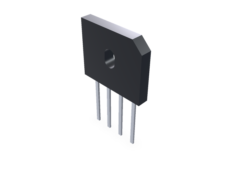
Single-phase bridge rectifiers in Vishay's through-hole cases: GBL, GBU, KBL and KBU in-line, KBPC1 and KBPC6 square, from Vishay's data sheets.
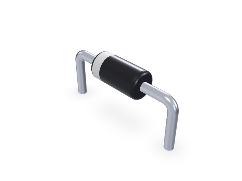
Axial leaded diodes in Vishay's DO-35, DO-41, DO-15, DO-201AD and P600 packages, with the cathode band, horizontal or vertical.
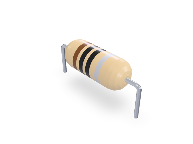
Axial leaded inductor, Fastron fixed choke coils (MICC, SMCC, MECC, HCCC, LACC, HBCC, VHBCC, XHBCC) and suppression coils (MISC, MESC, 77A), Vishay Dale molded IM-1 to IM-10, horizontal or vertical.