
STEVEMIT
steve/melf-resistor
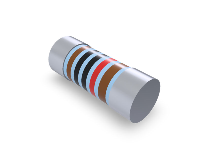
Thin film MELF resistors, Vishay Beyschlag MMU 0102 (MicroMELF), MMA 0204 (MiniMELF) and MMB 0207 (MELF), with colour rings.
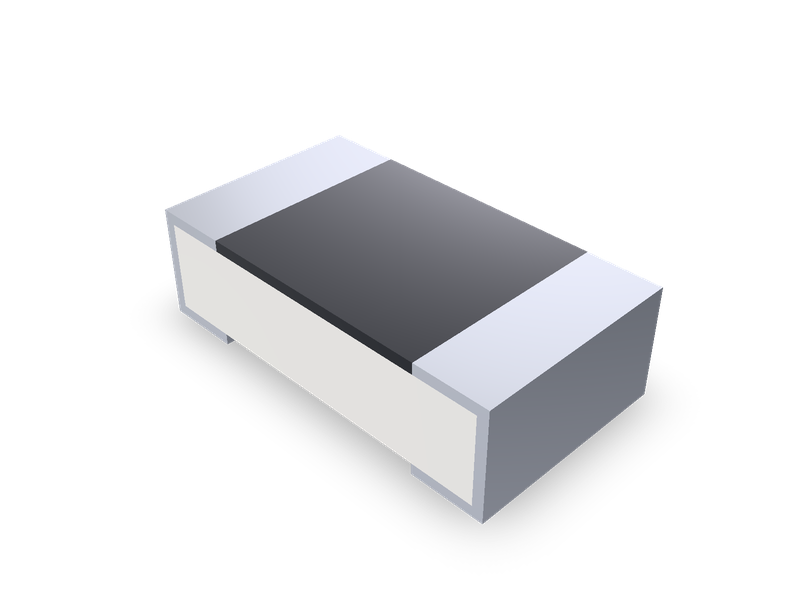
Thick film chip resistors, Vishay D/CRCW e3 sizes 0402 to 2512: alumina body, overcoat and wrap-around terminations.
| 1 | """Thick film chip resistor, Vishay D/CRCW e3 sizes 0402 to 2512. Centred on the origin, lying on the XY plane with its length along X: the |
| 2 | alumina body, the overcoat on top between the terminations, and a wrap-around termination at each end (each its own solid). Dimensions from |
| 3 | Vishay's data sheet; see the README.""" |
| 4 | from steve import Model |
| 5 | |
| 6 | size = "0603" # case size, inch code |
| 7 | |
| 8 | # size: (length L, width W, height H, bottom termination T1, top termination T2, mass in mg), nominal values in mm. |
| 9 | # Vishay, "D/CRCW e3, Standard Thick Film Chip Resistors", document 20035, revision 14-Apr-2026 |
| 10 | # (https://www.vishay.com/docs/20035/dcrcwe3.pdf), page 11, "DIMENSIONS AND MASS" table. |
| 11 | # 0603's L is 1.55 +0.10/-0.05; the others' are the stated nominal. |
| 12 | SIZES = { |
| 13 | "0402": (1.0, 0.5, 0.35, 0.25, 0.2, 0.65), |
| 14 | "0603": (1.55, 0.85, 0.45, 0.3, 0.3, 2.0), |
| 15 | "0805": (2.0, 1.25, 0.5, 0.3, 0.3, 5.5), |
| 16 | "1206": (3.2, 1.6, 0.55, 0.45, 0.4, 10.0), |
| 17 | "1210": (3.2, 2.5, 0.55, 0.45, 0.4, 16.0), |
| 18 | "1218": (3.2, 4.6, 0.55, 0.45, 0.4, 29.5), |
| 19 | "2010": (5.0, 2.5, 0.6, 0.6, 0.6, 25.5), |
| 20 | "2512": (6.3, 3.15, 0.6, 0.6, 0.6, 40.5), |
| 21 | } |
| 22 | # Proportion, for looks: the terminations' and the overcoat's thickness, 0.1 x H (the data sheet doesn't dimension it). |
| 23 | SKIN = 0.1 |
| 24 | |
| 25 | L, W, H, T1, T2, _mass = SIZES[size] |
| 26 | t = SKIN * H |
| 27 | model = Model() |
| 28 | # The alumina body inside the terminations and under the overcoat. |
| 29 | model.box("body", L - 2 * t, W, H - 2 * t, at=(0, 0, H / 2), op="new", body="body_body", name="Body") |
| 30 | # The overcoat on top between the terminations' top bands. |
| 31 | model.box("overcoat", L - 2 * T2, W, t, at=(0, 0, H - t / 2), op="new", body="overcoat_body", name="Overcoat") |
| 32 | # Each termination: its section in the XZ plane (bottom band T1 long, the end face, the top band T2 long), extruded across the width. |
| 33 | for tag, side in (("left", -1), ("right", 1)): |
| 34 | x_end = side * L / 2 |
| 35 | section = [(x_end, 0.0), (x_end - side * T1, 0.0), (x_end - side * T1, t), (x_end - side * t, t), (x_end - side * t, H - t), |
| 36 | (x_end - side * T2, H - t), (x_end - side * T2, H), (x_end, H)] |
| 37 | # The XZ plane's normal is -Y: offset -W/2 puts it on the +Y face, and the extrusion runs across the width to -Y. |
| 38 | model.plane(f"{tag}_plane", on="XZ", offset=-W / 2, name="Terminations") |
| 39 | with model.sketch(f"{tag}_sketch", on=f"{tag}_plane", name="Terminations") as sk: |
| 40 | sk.polyline(f"{tag}_section", section, closed=True) |
| 41 | model.extrude(f"{tag}_term", f"{tag}_sketch", distance=W, op="new", body=f"{tag}_body", name="Terminations") |
| 42 | # Materials, for looks and a rough mass: the substrate is alumina; the overcoat is glass and epoxy, ptfe (2.07) the nearest in the material |
| 43 | # list; the terminations are nickel barrier under matte tin (the "e3" finish), shown as tin. |
| 44 | model.material("alumina", bodies=["body_body"], color="#f2efe6") |
| 45 | model.material("ptfe", bodies=["overcoat_body"], color="#1f2124") |
| 46 | model.material("tin", bodies=["left_body", "right_body"], color="#c9ccd1") |
| 47 | result = model.result() |
| 48 |
| 1 | name = "steve/chip-resistor" |
| 2 | version = "1.0.0" |
| 3 | runtime = "steve" |
| 4 | license = "MIT" |
| 5 | summary = "Thick film chip resistors, Vishay D/CRCW e3 sizes 0402 to 2512: alumina body, overcoat and wrap-around terminations." |
| 6 | description = """Thick film chip resistors for board layouts and enclosures, in the EIA case sizes 0402, 0603, 0805, 1206, 1210, 1218, 2010 and 2512: the alumina body, the overcoat on top and the two wrap-around terminations, each its own solid. Length, width, height and the terminations' top and bottom lengths from Vishay's D/CRCW e3 data sheet. See the README.""" |
| 7 | tags = ["resistor", "chip-resistor", "smd", "passive", "electronics"] |
| 8 | |
| 9 | [parameters.size] |
| 10 | type = "choice" |
| 11 | default = "0603" |
| 12 | choices = ["0402", "0603", "0805", "1206", "1210", "1218", "2010", "2512"] |
| 13 | label = "Case size (inch)" |
| 14 | |
| 15 | [[presets]] |
| 16 | id = "0402" |
| 17 | title = "Chip resistor 0402 (1005 metric), 1 x 0.5 x 0.35 mm, Vishay D10/CRCW0402 e3" |
| 18 | params = { size = "0402" } |
| 19 | aliases = ["0402 resistor", "1005 metric resistor", "chip resistor 0402", "CRCW0402"] |
| 20 | standard = "Vishay D/CRCW e3" |
| 21 | |
| 22 | [[presets]] |
| 23 | id = "0603" |
| 24 | title = "Chip resistor 0603 (1608 metric), 1.55 x 0.85 x 0.45 mm, Vishay D11/CRCW0603 e3" |
| 25 | params = { size = "0603" } |
| 26 | aliases = ["0603 resistor", "1608 metric resistor", "chip resistor 0603", "CRCW0603"] |
| 27 | standard = "Vishay D/CRCW e3" |
| 28 | |
| 29 | [[presets]] |
| 30 | id = "0805" |
| 31 | title = "Chip resistor 0805 (2012 metric), 2 x 1.25 x 0.5 mm, Vishay D12/CRCW0805 e3" |
| 32 | params = { size = "0805" } |
| 33 | aliases = ["0805 resistor", "2012 metric resistor", "chip resistor 0805", "CRCW0805"] |
| 34 | standard = "Vishay D/CRCW e3" |
| 35 | |
| 36 | [[presets]] |
| 37 | id = "1206" |
| 38 | title = "Chip resistor 1206 (3216 metric), 3.2 x 1.6 x 0.55 mm, Vishay D25/CRCW1206 e3" |
| 39 | params = { size = "1206" } |
| 40 | aliases = ["1206 resistor", "3216 metric resistor", "chip resistor 1206", "CRCW1206"] |
| 41 | standard = "Vishay D/CRCW e3" |
| 42 | |
| 43 | [[presets]] |
| 44 | id = "1210" |
| 45 | title = "Chip resistor 1210 (3225 metric), 3.2 x 2.5 x 0.55 mm, Vishay CRCW1210 e3" |
| 46 | params = { size = "1210" } |
| 47 | aliases = ["1210 resistor", "3225 metric resistor", "chip resistor 1210", "CRCW1210"] |
| 48 | standard = "Vishay D/CRCW e3" |
| 49 | |
| 50 | [[presets]] |
| 51 | id = "1218" |
| 52 | title = "Chip resistor 1218 (3246 metric), 3.2 x 4.6 x 0.55 mm, Vishay CRCW1218 e3" |
| 53 | params = { size = "1218" } |
| 54 | aliases = ["1218 resistor", "3246 metric resistor", "chip resistor 1218", "CRCW1218"] |
| 55 | standard = "Vishay D/CRCW e3" |
| 56 | |
| 57 | [[presets]] |
| 58 | id = "2010" |
| 59 | title = "Chip resistor 2010 (5025 metric), 5 x 2.5 x 0.6 mm, Vishay CRCW2010 e3" |
| 60 | params = { size = "2010" } |
| 61 | aliases = ["2010 resistor", "5025 metric resistor", "chip resistor 2010", "CRCW2010"] |
| 62 | standard = "Vishay D/CRCW e3" |
| 63 | |
| 64 | [[presets]] |
| 65 | id = "2512" |
| 66 | title = "Chip resistor 2512 (6332 metric), 6.3 x 3.15 x 0.6 mm, Vishay CRCW2512 e3" |
| 67 | params = { size = "2512" } |
| 68 | aliases = ["2512 resistor", "6332 metric resistor", "chip resistor 2512", "CRCW2512"] |
| 69 | standard = "Vishay D/CRCW e3" |
| 70 |
Thick film chip resistors in the EIA case sizes 0402 to 2512, as Vishay's D/CRCW e3 series. The chip is centred on the origin, lying on the XY plane with its length along X. It is the alumina body, the overcoat on top between the terminations, and a wrap-around termination at each end: a band T1 long underneath, the end face, and a band T2 long on top. Each termination is its own solid.
Vishay, "D/CRCW e3, Standard Thick Film Chip Resistors", document number 20035, revision 14-Apr-2026, https://www.vishay.com/docs/20035/dcrcwe3.pdf, page 11, "DIMENSIONS AND MASS":
| Size | Vishay type | L | W | H | T1 | T2 | Mass |
|---|---|---|---|---|---|---|---|
| 0402 | D10/CRCW0402 e3 | 1.0 ± 0.05 | 0.5 ± 0.05 | 0.35 ± 0.05 | 0.25 ± 0.10 | 0.2 ± 0.10 | 0.65 mg |
| 0603 | D11/CRCW0603 e3 | 1.55 +0.10/-0.05 | 0.85 ± 0.10 | 0.45 ± 0.05 | 0.3 ± 0.20 | 0.3 ± 0.20 | 2 mg |
| 0805 | D12/CRCW0805 e3 | 2.0 +0.20/-0.10 | 1.25 ± 0.15 | 0.5 ± 0.10 | 0.3 +0.20/-0.10 | 0.3 ± 0.20 | 5.5 mg |
| 1206 | D25/CRCW1206 e3 | 3.2 +0.10/-0.20 | 1.6 ± 0.15 | 0.55 ± 0.05 | 0.45 ± 0.20 | 0.4 ± 0.20 | 10 mg |
| 1210 | CRCW1210 e3 | 3.2 ± 0.20 | 2.5 ± 0.20 | 0.55 ± 0.05 | 0.45 ± 0.20 | 0.4 ± 0.20 | 16 mg |
| 1218 | CRCW1218 e3 | 3.2 +0.10/-0.20 | 4.6 ± 0.15 | 0.55 ± 0.05 | 0.45 ± 0.20 | 0.4 ± 0.20 | 29.5 mg |
| 2010 | CRCW2010 e3 | 5.0 ± 0.15 | 2.5 ± 0.15 | 0.6 ± 0.10 | 0.6 ± 0.20 | 0.6 ± 0.20 | 25.5 mg |
| 2512 | CRCW2512 e3 | 6.3 ± 0.20 | 3.15 ± 0.15 | 0.6 ± 0.10 | 0.6 ± 0.20 | 0.6 ± 0.20 | 40.5 mg |
The model uses the nominal values. L is the length, W the width, H the height, T1 the termination's length underneath and T2 its length on top.
Proportions, stated plainly. The data sheet doesn't dimension the terminations' thickness or the overcoat's. Both are drawn 0.1 x H thick, and the alumina body fills the rest. The bottom between the terminations' bands is left open by that thickness, so the chip stands on its terminations.
Materials, for looks and a rough mass: the substrate is alumina (4.0). The overcoat is glass and epoxy, and ptfe (2.07) is the nearest in the material list. The terminations are a nickel barrier under matte tin (the "e3" finish), shown as tin (7.28). The model's mass against Vishay's:
| Size | Model | Vishay | |
|---|---|---|---|
| 0402 | 0.73 mg | 0.65 mg | +12 % |
| 0603 | 2.40 mg | 2 mg | +20 % |
| 0805 | 4.89 mg | 5.5 mg | -11 % |
| 1206 | 10.79 mg | 10 mg | +8 % |
| 1210 | 16.86 mg | 16 mg | +5 % |
| 1218 | 31.03 mg | 29.5 mg | +5 % |
| 2010 | 28.27 mg | 25.5 mg | +11 % |
| 2512 | 44.00 mg | 40.5 mg | +9 % |
The old catalogue's R_<inch>_<metric>Metric entries have no models to measure. The metric code is the case's length and width rounded to 0.1 mm, so a name maps to Vishay's chip of that inch size when Vishay's nominal length and width are within 0.05 mm of the code. All eight do. 0603 (1608) is 1.55 x 0.85, 0805 (2012) 2.0 x 1.25, 1218 (3246) 3.2 x 4.6 and 2512 (6332) 6.3 x 3.15. The others are the code exactly.
Not mapped yet, because D/CRCW e3 doesn't have them: 01005, 0201, 0612, 0815, 1020, 1806, 1812, 2816 and 4020. The resistor arrays, MELF resistors and current shunts in the same catalogue family aren't read yet either; see COVERAGE.md.
| 1 | # Chip resistor |
| 2 | |
| 3 | Thick film chip resistors in the EIA case sizes 0402 to 2512, as Vishay's D/CRCW e3 series. The chip is centred on the origin, lying on the XY plane with its length along X. It is the alumina body, the overcoat on top between the terminations, and a wrap-around termination at each end: a band T1 long underneath, the end face, and a band T2 long on top. Each termination is its own solid. |
| 4 | |
| 5 | ## Source |
| 6 | |
| 7 | Vishay, "D/CRCW e3, Standard Thick Film Chip Resistors", document number 20035, revision 14-Apr-2026, <https://www.vishay.com/docs/20035/dcrcwe3.pdf>, page 11, "DIMENSIONS AND MASS": |
| 8 | |
| 9 | | Size | Vishay type | L | W | H | T1 | T2 | Mass | |
| 10 | |---|---|---|---|---|---|---|---| |
| 11 | | 0402 | D10/CRCW0402 e3 | 1.0 ± 0.05 | 0.5 ± 0.05 | 0.35 ± 0.05 | 0.25 ± 0.10 | 0.2 ± 0.10 | 0.65 mg | |
| 12 | | 0603 | D11/CRCW0603 e3 | 1.55 +0.10/-0.05 | 0.85 ± 0.10 | 0.45 ± 0.05 | 0.3 ± 0.20 | 0.3 ± 0.20 | 2 mg | |
| 13 | | 0805 | D12/CRCW0805 e3 | 2.0 +0.20/-0.10 | 1.25 ± 0.15 | 0.5 ± 0.10 | 0.3 +0.20/-0.10 | 0.3 ± 0.20 | 5.5 mg | |
| 14 | | 1206 | D25/CRCW1206 e3 | 3.2 +0.10/-0.20 | 1.6 ± 0.15 | 0.55 ± 0.05 | 0.45 ± 0.20 | 0.4 ± 0.20 | 10 mg | |
| 15 | | 1210 | CRCW1210 e3 | 3.2 ± 0.20 | 2.5 ± 0.20 | 0.55 ± 0.05 | 0.45 ± 0.20 | 0.4 ± 0.20 | 16 mg | |
| 16 | | 1218 | CRCW1218 e3 | 3.2 +0.10/-0.20 | 4.6 ± 0.15 | 0.55 ± 0.05 | 0.45 ± 0.20 | 0.4 ± 0.20 | 29.5 mg | |
| 17 | | 2010 | CRCW2010 e3 | 5.0 ± 0.15 | 2.5 ± 0.15 | 0.6 ± 0.10 | 0.6 ± 0.20 | 0.6 ± 0.20 | 25.5 mg | |
| 18 | | 2512 | CRCW2512 e3 | 6.3 ± 0.20 | 3.15 ± 0.15 | 0.6 ± 0.10 | 0.6 ± 0.20 | 0.6 ± 0.20 | 40.5 mg | |
| 19 | |
| 20 | The model uses the nominal values. L is the length, W the width, H the height, T1 the termination's length underneath and T2 its length on top. |
| 21 | |
| 22 | **Proportions, stated plainly.** The data sheet doesn't dimension the terminations' thickness or the overcoat's. Both are drawn 0.1 x H thick, and the alumina body fills the rest. The bottom between the terminations' bands is left open by that thickness, so the chip stands on its terminations. |
| 23 | |
| 24 | **Materials**, for looks and a rough mass: the substrate is alumina (4.0). The overcoat is glass and epoxy, and ptfe (2.07) is the nearest in the material list. The terminations are a nickel barrier under matte tin (the "e3" finish), shown as tin (7.28). The model's mass against Vishay's: |
| 25 | |
| 26 | | Size | Model | Vishay | | |
| 27 | |---|---|---|---| |
| 28 | | 0402 | 0.73 mg | 0.65 mg | +12 % | |
| 29 | | 0603 | 2.40 mg | 2 mg | +20 % | |
| 30 | | 0805 | 4.89 mg | 5.5 mg | -11 % | |
| 31 | | 1206 | 10.79 mg | 10 mg | +8 % | |
| 32 | | 1210 | 16.86 mg | 16 mg | +5 % | |
| 33 | | 1218 | 31.03 mg | 29.5 mg | +5 % | |
| 34 | | 2010 | 28.27 mg | 25.5 mg | +11 % | |
| 35 | | 2512 | 44.00 mg | 40.5 mg | +9 % | |
| 36 | |
| 37 | ## Catalogue models |
| 38 | |
| 39 | The old catalogue's `R_<inch>_<metric>Metric` entries have no models to measure. The metric code is the case's length and width rounded to 0.1 mm, so a name maps to Vishay's chip of that inch size when Vishay's nominal length and width are within 0.05 mm of the code. All eight do. 0603 (1608) is 1.55 x 0.85, 0805 (2012) 2.0 x 1.25, 1218 (3246) 3.2 x 4.6 and 2512 (6332) 6.3 x 3.15. The others are the code exactly. |
| 40 | |
| 41 | Not mapped yet, because D/CRCW e3 doesn't have them: 01005, 0201, 0612, 0815, 1020, 1806, 1812, 2816 and 4020. The resistor arrays, MELF resistors and current shunts in the same catalogue family aren't read yet either; see `COVERAGE.md`. |
| 42 |
Thick film chip resistors for board layouts and enclosures, in the EIA case sizes 0402, 0603, 0805, 1206, 1210, 1218, 2010 and 2512: the alumina body, the overcoat on top and the two wrap-around terminations, each its own solid. Length, width, height and the terminations' top and bottom lengths from Vishay's D/CRCW e3 data sheet. See the README.
Thick film chip resistors in the EIA case sizes 0402 to 2512, as Vishay's D/CRCW e3 series. The chip is centred on the origin, lying on the XY plane with its length along X. It is the alumina body, the overcoat on top between the terminations, and a wrap-around termination at each end: a band T1 long underneath, the end face, and a band T2 long on top. Each termination is its own solid.
Vishay, "D/CRCW e3, Standard Thick Film Chip Resistors", document number 20035, revision 14-Apr-2026, https://www.vishay.com/docs/20035/dcrcwe3.pdf, page 11, "DIMENSIONS AND MASS":
| Size | Vishay type | L | W | H | T1 | T2 | Mass |
|---|---|---|---|---|---|---|---|
| 0402 | D10/CRCW0402 e3 | 1.0 ± 0.05 | 0.5 ± 0.05 | 0.35 ± 0.05 | 0.25 ± 0.10 | 0.2 ± 0.10 | 0.65 mg |
| 0603 | D11/CRCW0603 e3 | 1.55 +0.10/-0.05 | 0.85 ± 0.10 | 0.45 ± 0.05 | 0.3 ± 0.20 | 0.3 ± 0.20 | 2 mg |
| 0805 | D12/CRCW0805 e3 | 2.0 +0.20/-0.10 | 1.25 ± 0.15 | 0.5 ± 0.10 | 0.3 +0.20/-0.10 | 0.3 ± 0.20 | 5.5 mg |
| 1206 | D25/CRCW1206 e3 | 3.2 +0.10/-0.20 | 1.6 ± 0.15 | 0.55 ± 0.05 | 0.45 ± 0.20 | 0.4 ± 0.20 | 10 mg |
| 1210 | CRCW1210 e3 | 3.2 ± 0.20 | 2.5 ± 0.20 | 0.55 ± 0.05 | 0.45 ± 0.20 | 0.4 ± 0.20 | 16 mg |
| 1218 | CRCW1218 e3 | 3.2 +0.10/-0.20 | 4.6 ± 0.15 | 0.55 ± 0.05 | 0.45 ± 0.20 | 0.4 ± 0.20 | 29.5 mg |
| 2010 | CRCW2010 e3 | 5.0 ± 0.15 | 2.5 ± 0.15 | 0.6 ± 0.10 | 0.6 ± 0.20 | 0.6 ± 0.20 | 25.5 mg |
| 2512 | CRCW2512 e3 | 6.3 ± 0.20 | 3.15 ± 0.15 | 0.6 ± 0.10 | 0.6 ± 0.20 | 0.6 ± 0.20 | 40.5 mg |
The model uses the nominal values. L is the length, W the width, H the height, T1 the termination's length underneath and T2 its length on top.
Proportions, stated plainly. The data sheet doesn't dimension the terminations' thickness or the overcoat's. Both are drawn 0.1 x H thick, and the alumina body fills the rest. The bottom between the terminations' bands is left open by that thickness, so the chip stands on its terminations.
Materials, for looks and a rough mass: the substrate is alumina (4.0). The overcoat is glass and epoxy, and ptfe (2.07) is the nearest in the material list. The terminations are a nickel barrier under matte tin (the "e3" finish), shown as tin (7.28). The model's mass against Vishay's:
| Size | Model | Vishay | |
|---|---|---|---|
| 0402 | 0.73 mg | 0.65 mg | +12 % |
| 0603 | 2.40 mg | 2 mg | +20 % |
| 0805 | 4.89 mg | 5.5 mg | -11 % |
| 1206 | 10.79 mg | 10 mg | +8 % |
| 1210 | 16.86 mg | 16 mg | +5 % |
| 1218 | 31.03 mg | 29.5 mg | +5 % |
| 2010 | 28.27 mg | 25.5 mg | +11 % |
| 2512 | 44.00 mg | 40.5 mg | +9 % |
The old catalogue's R_<inch>_<metric>Metric entries have no models to measure. The metric code is the case's length and width rounded to 0.1 mm, so a name maps to Vishay's chip of that inch size when Vishay's nominal length and width are within 0.05 mm of the code. All eight do. 0603 (1608) is 1.55 x 0.85, 0805 (2012) 2.0 x 1.25, 1218 (3246) 3.2 x 4.6 and 2512 (6332) 6.3 x 3.15. The others are the code exactly.
Not mapped yet, because D/CRCW e3 doesn't have them: 01005, 0201, 0612, 0815, 1020, 1806, 1812, 2816 and 4020. The resistor arrays, MELF resistors and current shunts in the same catalogue family aren't read yet either; see COVERAGE.md.
Thin film MELF resistors, Vishay Beyschlag MMU 0102 (MicroMELF), MMA 0204 (MiniMELF) and MMB 0207 (MELF), with colour rings.
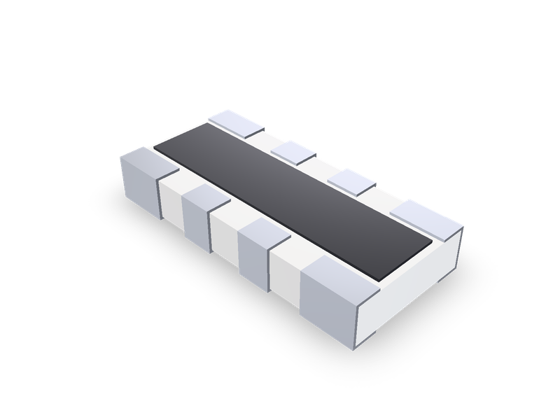
Thick film chip resistor arrays with convex terminals, Vishay CRA04S (0402), CRA06E/S (0603) and CRA12E/S (1206), 4 to 10 terminals.
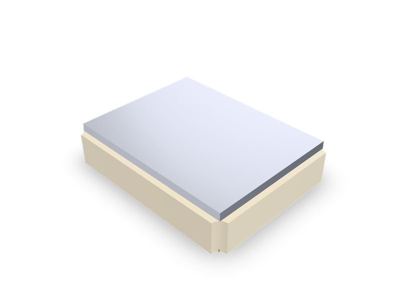
SMD quartz crystals by maker series: Epson FA-238, FA-238V, TSX-3225, MA-406, MA-505; TXC 7M, AX; Abracon ABM8G, ABM3B; EuroQuartz MT.
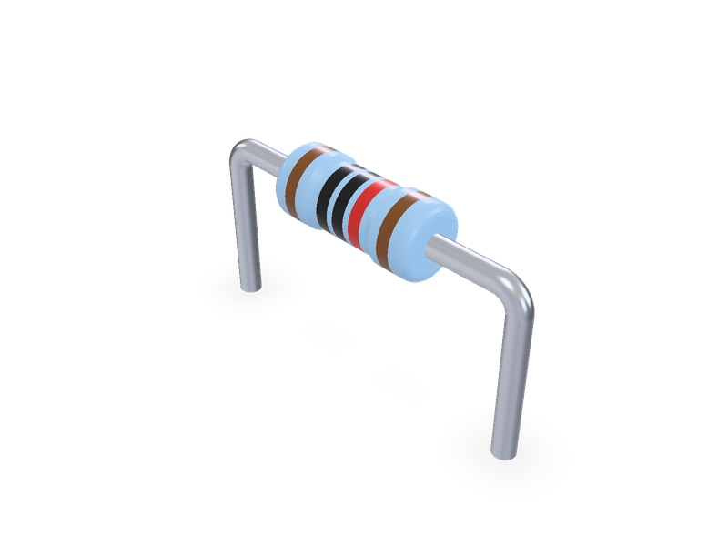
Axial leaded metal film resistor, Vishay Beyschlag MBA/SMA 0204, MBB/SMA 0207 and MBE/SMA 0414, with colour rings, horizontal or vertical.