
STEVEMIT
steve/melf-diode
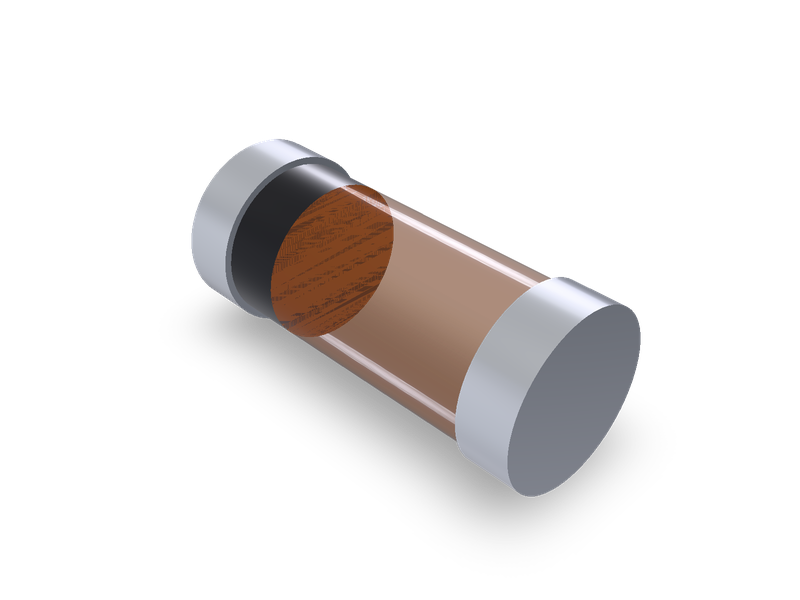
Surface-mount diode packages MELF (DO-213AB), MiniMELF (SOD-80) and MicroMELF, from Vishay's package drawings.
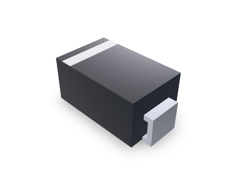
Surface-mount diode packages DO-214AC (SMA), DO-214AA (SMB) and DO-214AB (SMC), from Vishay's outline drawings.
| 1 | """Surface-mount diode in a DO-214 package (SMA, SMB, SMC), by Vishay's outline drawings. Centred on the origin with the seating plane on the |
| 2 | XY plane and the length along X: the moulded body, the cathode band on top at the -X end, and a J-bend lead at each end that wraps under the |
| 3 | body (each lead its own solid). Dimensions from Vishay's outline drawings; see the README.""" |
| 4 | from steve import Model |
| 5 | |
| 6 | package = "SMA" # DO-214AC (SMA), DO-214AA (SMB) or DO-214AB (SMC) |
| 7 | |
| 8 | # package: (JEDEC outline, body length, body width, lead width, height, lead thickness, foot under the body, length over the leads, |
| 9 | # standoff under the body), ranges (min, max) in mm. |
| 10 | # Vishay Semiconductors outline drawings, "DIMENSIONS in inches (millimeters)", revision 09-Jul-10: |
| 11 | # SMA document 95400 (https://www.vishay.com/docs/95400/sma.pdf), SMB 95401 (.../95401/smb.pdf), SMC 95402 (.../95402/smc.pdf). |
| 12 | OUTLINES = { |
| 13 | "SMA": ("DO-214AC", (3.99, 4.50), (2.54, 2.79), (1.25, 1.65), (1.98, 2.29), (0.152, 0.305), (0.76, 1.52), (4.93, 5.28), (0.0, 0.203)), |
| 14 | "SMB": ("DO-214AA", (4.06, 4.57), (3.30, 3.94), (1.95, 2.20), (2.13, 2.44), (0.152, 0.305), (0.76, 1.52), (5.21, 5.59), (0.0, 0.2)), |
| 15 | "SMC": ("DO-214AB", (6.60, 7.11), (5.59, 6.22), (2.90, 3.20), (2.06, 2.62), (0.152, 0.305), (0.76, 1.52), (7.75, 8.13), (0.0, 0.2)), |
| 16 | } |
| 17 | # Proportions, for looks (the drawings show these but don't dimension them): the lead leaves the body at half the height; the cathode band |
| 18 | # is 0.12 of the body's length wide, 0.1 of it in from the -X end, and 0.03 proud of the top. |
| 19 | ARM = 0.5 |
| 20 | BAND_W = 0.12 |
| 21 | BAND_IN = 0.1 |
| 22 | BAND_T = 0.03 |
| 23 | |
| 24 | |
| 25 | def mid(pair): |
| 26 | return (pair[0] + pair[1]) / 2 |
| 27 | |
| 28 | |
| 29 | jedec, BL, BW, LW, HT, LT, FOOT, SPAN, STAND = OUTLINES[package] |
| 30 | body_l, body_w, lead_w, height, t, foot, span, standoff = (mid(v) for v in (BL, BW, LW, HT, LT, FOOT, SPAN, STAND)) |
| 31 | model = Model() |
| 32 | model.box("body", body_l, body_w, height - standoff, at=(0, 0, (height + standoff) / 2), op="new", body="body_body", name="Body") |
| 33 | model.box("band", BAND_W * body_l, body_w, BAND_T, at=(-body_l / 2 + (BAND_IN + BAND_W / 2) * body_l, 0, height + BAND_T / 2), op="new", |
| 34 | body="band_body", name="Cathode band") |
| 35 | arm_z = ARM * height |
| 36 | leads = [] |
| 37 | for tag, side in (("cathode", -1), ("anode", 1)): |
| 38 | inner, face, out = side * (body_l / 2 - 0.3), side * body_l / 2, side * span / 2 |
| 39 | tip = out - side * foot |
| 40 | # The lead's side section (x, z): out of the body's end at arm_z, down the outside, and under the body to the foot's inner end. |
| 41 | section = [(inner, arm_z + t), (out, arm_z + t), (out, 0.0), (tip, 0.0), (tip, t), (out - side * t, t), (out - side * t, arm_z), |
| 42 | (inner, arm_z)] |
| 43 | # The XZ plane's normal is -Y: offset -lead_w / 2 puts it on the lead's +Y side, and the extrusion runs across the lead to -Y. |
| 44 | model.plane(f"{tag}_plane", on="XZ", offset=-lead_w / 2, name="Leads") |
| 45 | with model.sketch(f"{tag}_sketch", on=f"{tag}_plane", name="Leads") as sk: |
| 46 | sk.polyline(f"{tag}_section", section, closed=True) |
| 47 | model.extrude(f"{tag}_lead", f"{tag}_sketch", distance=lead_w, op="new", body=f"{tag}_body", name="Leads") |
| 48 | leads.append(f"{tag}_body") |
| 49 | # The leads run into the body by 0.3, and their feet tuck under it in a recess: cut that room out of the body, so that no solids overlap. |
| 50 | with model.sketch("room_sketch", on="cathode_plane", name="Room for the leads") as sk: |
| 51 | for tag, side in (("cathode", -1), ("anode", 1)): |
| 52 | a, b = side * (body_l / 2 - 0.3), side * body_l / 2 |
| 53 | sk.rect(f"room_{tag}", (min(a, b), arm_z), (max(a, b), arm_z + t)) |
| 54 | c = side * (span / 2 - foot) |
| 55 | sk.rect(f"recess_{tag}", (min(c, b), 0.0), (max(c, b), t)) |
| 56 | model.extrude("room", "room_sketch", distance=lead_w, op="cut", body="body_body", name="Room for the leads") |
| 57 | # Materials, for looks and a rough mass: the moulding is epoxy compound, mostly silica filler (density about 1.9 to 2.0), ptfe (2.07) the |
| 58 | # nearest in the material list; the leads are tin-plated copper, copper; the band is marking ink, shown in ptfe. |
| 59 | model.material("ptfe", bodies=["body_body"], color="#26282b") |
| 60 | model.material("ptfe", bodies=["band_body"], color="#c8c8c4") |
| 61 | model.material("copper", bodies=leads, color="#c9ccd1") |
| 62 | result = model.result() |
| 63 |
| 1 | name = "steve/do214-diode" |
| 2 | version = "1.0.0" |
| 3 | runtime = "steve" |
| 4 | license = "MIT" |
| 5 | summary = "Surface-mount diode packages DO-214AC (SMA), DO-214AA (SMB) and DO-214AB (SMC), from Vishay's outline drawings." |
| 6 | description = """Surface-mount diode packages for board layouts and enclosures: the moulded body, the cathode band and the two J-bend leads that wrap under the body, each lead its own solid, in the DO-214AC (SMA), DO-214AA (SMB) and DO-214AB (SMC) outlines. Dimensions from Vishay's outline drawings. See the README.""" |
| 7 | tags = ["diode", "smd", "sma", "smb", "smc", "do-214", "electronics"] |
| 8 | |
| 9 | [parameters.package] |
| 10 | type = "choice" |
| 11 | default = "SMA" |
| 12 | choices = ["SMA", "SMB", "SMC"] |
| 13 | label = "Package" |
| 14 | description = "SMA: DO-214AC. SMB: DO-214AA. SMC: DO-214AB." |
| 15 | |
| 16 | [[presets]] |
| 17 | id = "SMA" |
| 18 | title = "SMA (DO-214AC) diode package, Vishay outline" |
| 19 | params = { package = "SMA" } |
| 20 | aliases = ["DO-214AC", "SMA diode", "DO-214AC (SMA)"] |
| 21 | standard = "Vishay outline" |
| 22 | |
| 23 | [[presets]] |
| 24 | id = "SMB" |
| 25 | title = "SMB (DO-214AA) diode package, Vishay outline" |
| 26 | params = { package = "SMB" } |
| 27 | aliases = ["DO-214AA", "SMB diode", "DO-214AA (SMB)"] |
| 28 | standard = "Vishay outline" |
| 29 | |
| 30 | [[presets]] |
| 31 | id = "SMC" |
| 32 | title = "SMC (DO-214AB) diode package, Vishay outline" |
| 33 | params = { package = "SMC" } |
| 34 | aliases = ["DO-214AB", "SMC diode", "DO-214AB (SMC)"] |
| 35 | standard = "Vishay outline" |
| 36 |
Surface-mount diode packages DO-214AC (SMA), DO-214AA (SMB) and DO-214AB (SMC), as Vishay draws them. The package is centred on the origin with the seating plane on the XY plane and its length along X. It is the moulded body, the cathode band on top at the -X end, and a J-bend lead at each end. Each lead leaves the body's end, runs down the outside and tucks under the body. Each lead is its own solid.
Vishay Semiconductors outline drawings, "DIMENSIONS in inches (millimeters)", revision 09-Jul-10:
| Package | Body length | Body width | Lead width | Height | Lead thickness | Foot under the body | Over the leads | Standoff |
|---|---|---|---|---|---|---|---|---|
| SMA | 3.99–4.50 | 2.54–2.79 | 1.25–1.65 | 1.98–2.29 | 0.152–0.305 | 0.76–1.52 | 4.93–5.28 | 0–0.203 |
| SMB | 4.06–4.57 | 3.30–3.94 | 1.95–2.20 | 2.13–2.44 | 0.152–0.305 | 0.76–1.52 | 5.21–5.59 | 0–0.2 |
| SMC | 6.60–7.11 | 5.59–6.22 | 2.90–3.20 | 2.06–2.62 | 0.152–0.305 | 0.76–1.52 | 7.75–8.13 | 0–0.2 |
The model uses the middle of each range.
Proportions, stated plainly. The drawings show these but don't dimension them:
Materials, for looks and a rough mass. The moulding is epoxy compound, mostly silica filler (density about 1.9 to 2.0), and ptfe (2.07) is the nearest in the material list. The leads are tin-plated copper, shown as copper. The model weighs about 63 mg (SMA), 94 mg (SMB) and 222 mg (SMC). The outline drawings give no weight, so there is nothing to check this against.
The old catalogue's D_SMA, D_SMB and D_SMC entries have no models to measure. Each names the JEDEC package (SMA is DO-214AC, SMB DO-214AA and SMC DO-214AB), and each maps to Vishay's outline of that package.
The other surface-mount diode packages in the family (SOD, MELF, PowerDI and the others) aren't read yet; see COVERAGE.md.
| 1 | # DO-214 diode package |
| 2 | |
| 3 | Surface-mount diode packages DO-214AC (SMA), DO-214AA (SMB) and DO-214AB (SMC), as Vishay draws them. The package is centred on the origin with the seating plane on the XY plane and its length along X. It is the moulded body, the cathode band on top at the -X end, and a J-bend lead at each end. Each lead leaves the body's end, runs down the outside and tucks under the body. Each lead is its own solid. |
| 4 | |
| 5 | ## Source |
| 6 | |
| 7 | Vishay Semiconductors outline drawings, "DIMENSIONS in inches (millimeters)", revision 09-Jul-10: |
| 8 | |
| 9 | - SMA, DO-214AC: document number 95400, <https://www.vishay.com/docs/95400/sma.pdf>, page 1. |
| 10 | - SMB, DO-214AA: document number 95401, <https://www.vishay.com/docs/95401/smb.pdf>, page 1. |
| 11 | - SMC, DO-214AB: document number 95402, <https://www.vishay.com/docs/95402/smc.pdf>, page 1. |
| 12 | |
| 13 | | Package | Body length | Body width | Lead width | Height | Lead thickness | Foot under the body | Over the leads | Standoff | |
| 14 | |---|---|---|---|---|---|---|---|---| |
| 15 | | SMA | 3.99–4.50 | 2.54–2.79 | 1.25–1.65 | 1.98–2.29 | 0.152–0.305 | 0.76–1.52 | 4.93–5.28 | 0–0.203 | |
| 16 | | SMB | 4.06–4.57 | 3.30–3.94 | 1.95–2.20 | 2.13–2.44 | 0.152–0.305 | 0.76–1.52 | 5.21–5.59 | 0–0.2 | |
| 17 | | SMC | 6.60–7.11 | 5.59–6.22 | 2.90–3.20 | 2.06–2.62 | 0.152–0.305 | 0.76–1.52 | 7.75–8.13 | 0–0.2 | |
| 18 | |
| 19 | The model uses the middle of each range. |
| 20 | |
| 21 | **Proportions, stated plainly.** The drawings show these but don't dimension them: |
| 22 | |
| 23 | - The lead leaves the body at half its height, and runs 0.3 into the body. Its foot sits in a recess in the body's underside, so no solids overlap. |
| 24 | - The cathode band is 0.12 of the body's length wide, 0.1 of the length in from the -X end, and 0.03 proud of the top. The drawings mark the band but don't dimension it. |
| 25 | - The body is a plain block; the drawn draft of the moulding's top isn't modelled. |
| 26 | |
| 27 | **Materials**, for looks and a rough mass. The moulding is epoxy compound, mostly silica filler (density about 1.9 to 2.0), and ptfe (2.07) is the nearest in the material list. The leads are tin-plated copper, shown as copper. The model weighs about 63 mg (SMA), 94 mg (SMB) and 222 mg (SMC). The outline drawings give no weight, so there is nothing to check this against. |
| 28 | |
| 29 | ## Catalogue models |
| 30 | |
| 31 | The old catalogue's `D_SMA`, `D_SMB` and `D_SMC` entries have no models to measure. Each names the JEDEC package (SMA is DO-214AC, SMB DO-214AA and SMC DO-214AB), and each maps to Vishay's outline of that package. |
| 32 | |
| 33 | The other surface-mount diode packages in the family (SOD, MELF, PowerDI and the others) aren't read yet; see `COVERAGE.md`. |
| 34 |
Surface-mount diode packages for board layouts and enclosures: the moulded body, the cathode band and the two J-bend leads that wrap under the body, each lead its own solid, in the DO-214AC (SMA), DO-214AA (SMB) and DO-214AB (SMC) outlines. Dimensions from Vishay's outline drawings. See the README.
Surface-mount diode packages DO-214AC (SMA), DO-214AA (SMB) and DO-214AB (SMC), as Vishay draws them. The package is centred on the origin with the seating plane on the XY plane and its length along X. It is the moulded body, the cathode band on top at the -X end, and a J-bend lead at each end. Each lead leaves the body's end, runs down the outside and tucks under the body. Each lead is its own solid.
Vishay Semiconductors outline drawings, "DIMENSIONS in inches (millimeters)", revision 09-Jul-10:
| Package | Body length | Body width | Lead width | Height | Lead thickness | Foot under the body | Over the leads | Standoff |
|---|---|---|---|---|---|---|---|---|
| SMA | 3.99–4.50 | 2.54–2.79 | 1.25–1.65 | 1.98–2.29 | 0.152–0.305 | 0.76–1.52 | 4.93–5.28 | 0–0.203 |
| SMB | 4.06–4.57 | 3.30–3.94 | 1.95–2.20 | 2.13–2.44 | 0.152–0.305 | 0.76–1.52 | 5.21–5.59 | 0–0.2 |
| SMC | 6.60–7.11 | 5.59–6.22 | 2.90–3.20 | 2.06–2.62 | 0.152–0.305 | 0.76–1.52 | 7.75–8.13 | 0–0.2 |
The model uses the middle of each range.
Proportions, stated plainly. The drawings show these but don't dimension them:
Materials, for looks and a rough mass. The moulding is epoxy compound, mostly silica filler (density about 1.9 to 2.0), and ptfe (2.07) is the nearest in the material list. The leads are tin-plated copper, shown as copper. The model weighs about 63 mg (SMA), 94 mg (SMB) and 222 mg (SMC). The outline drawings give no weight, so there is nothing to check this against.
The old catalogue's D_SMA, D_SMB and D_SMC entries have no models to measure. Each names the JEDEC package (SMA is DO-214AC, SMB DO-214AA and SMC DO-214AB), and each maps to Vishay's outline of that package.
The other surface-mount diode packages in the family (SOD, MELF, PowerDI and the others) aren't read yet; see COVERAGE.md.
Surface-mount diode packages MELF (DO-213AB), MiniMELF (SOD-80) and MicroMELF, from Vishay's package drawings.
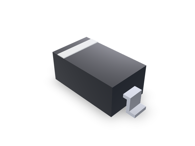
Surface-mount diode packages SOD-123, SOD-323, SOD-523 and SMF (DO-219AB), from Vishay's package drawings.
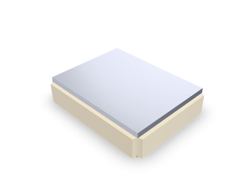
SMD quartz crystals by maker series: Epson FA-238, FA-238V, TSX-3225, MA-406, MA-505; TXC 7M, AX; Abracon ABM8G, ABM3B; EuroQuartz MT.
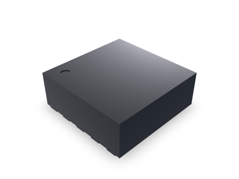
No-lead small-outline IC packages by TI outline: WSON-8/10/12/16, VSON-8 and X1SON-8, 0.4 to 0.8 mm pitch, with exposed thermal pad.